Method of manufacturing wiring substrate and method of manufacturing electronic component mounting structure

a technology of mounting structure and wiring substrate, which is applied in the direction of printed circuit manufacturing, printed circuit aspects, conductive pattern formation, etc., can solve the problems of cost increase and complicated steps, and achieve the effects of high reliability, high reliability, and easy transportation or handling of wiring substra

Active Publication Date: 2007-06-07
SHINKO ELECTRIC IND CO LTD
View PDF11 Cites 86 Cited by
  • Summary
  • Abstract
  • Description
  • Claims
  • Application Information

AI Technical Summary

Benefits of technology

[0017] Meanwhile, in a preferred mode in which an electronic component is mounted on the wiring substrate of the present invention, after obtaining the wiring member by separating the metal foil and the build-up layer thereon from the underlying layer, an electronic component is mounted on an upper surface of the wiring member while leaving the metal foil on a lower surface. Thereafter, the metal foil is removed from the wiring member to expose the lowermost wiring layer, which is used as the external connection pad. Since the metal foil functions as a reinforcing member, it becomes easy to convey or handle the wiring substrate without receiving an influence of warp rather than a case of mounting the electronic component after removing the metal foil. In this ...

Problems solved by technology

Accordingly, this step may be com...

Method used


Image

  • Method of manufacturing wiring substrate and method of manufacturing electronic component mounting structure
  • Method of manufacturing wiring substrate and method of manufacturing electronic component mounting structure
  • Method of manufacturing wiring substrate and method of manufacturing electronic component mounting structure

Examples


first embodiment

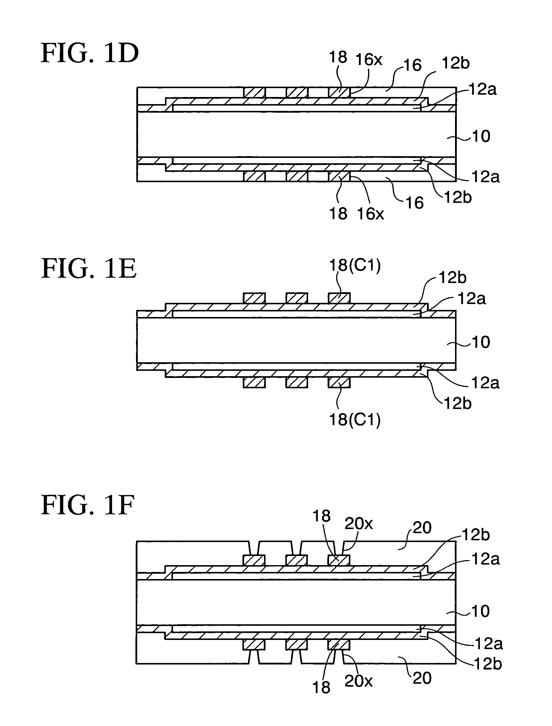
[0024]FIGS. 1A to 1L are cross-sectional views sequentially showing a method of manufacturing a wiring substrate according to a first embodiment of the present invention.

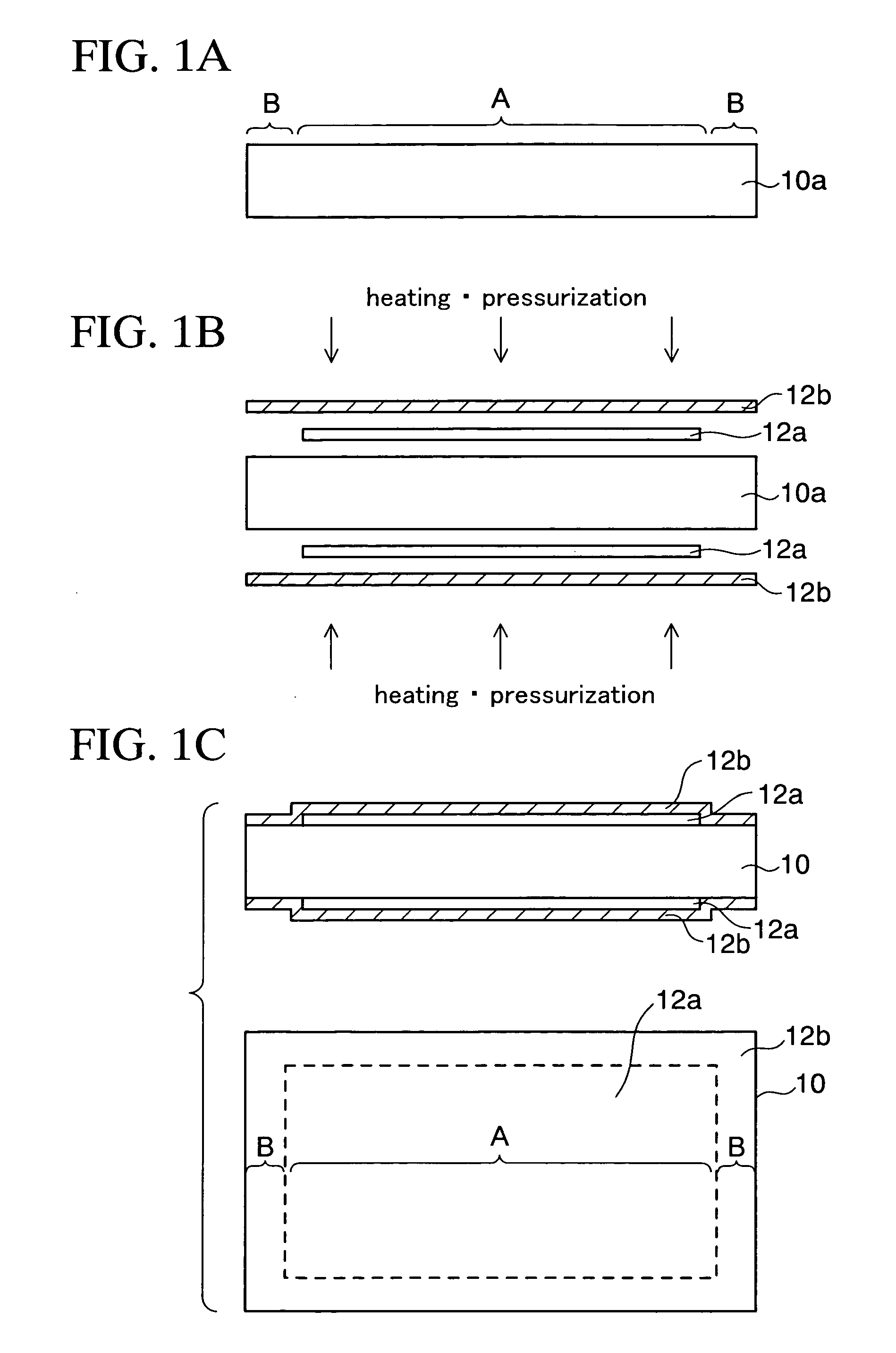
[0025] As shown in FIG. 1A, first, a prepreg 10a which is composed by impregnating a glass cloth (a woven fabric), a nonwoven glass fabric, aramide fibers or the like with resin such as epoxy resin is prepared. The prepreg 10a of the B-stage (in a semi-hardened state) is used hereto.

[0026] Wiring formation regions A and outer peripheral portions B on the outside of the wiring formation regions A are defined on both surfaces of the prepreg 10a. The wiring formation regions A may be defined one by one on the respective surfaces of the prepreg 10a or a plurality of regions may be defined thereon.

[0027] Thereafter, as shown in FIG. 1B, underlying layers 12a and copper foils 12b (metal foils) having a thickness in a range of 12 to 18 μm are prepared. As the underlying layer 12a, a metal foil such as a copper foil, a r...

second embodiment

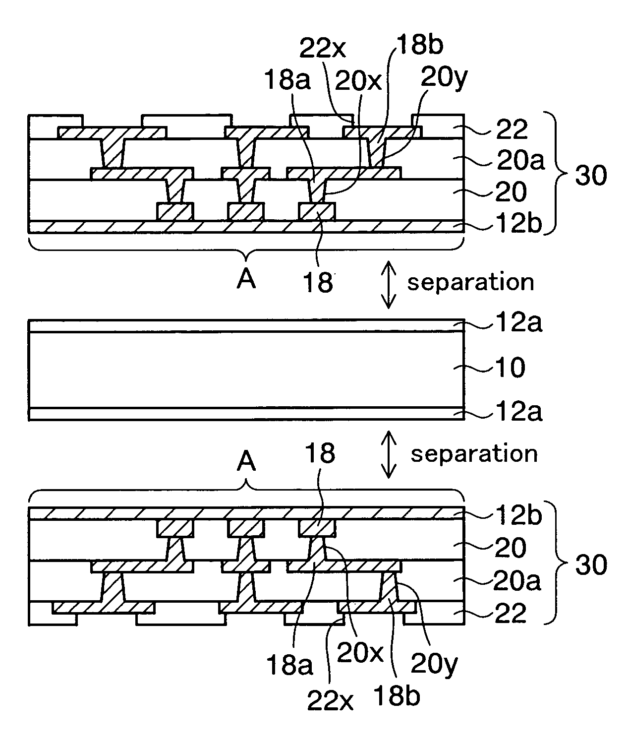
[0050]FIGS. 2A to 2F are cross-sectional views showing a method of manufacturing an electronic component mounting structure according to a second embodiment of the present invention. In the second embodiment, a preferred method of mounting an electronic component on a wiring substrate will be described on the basis of the technical idea of the method of manufacturing a wiring substrate of the present invention.

[0051] As shown in FIG. 2A, first, a structure in which underlying layers 12a and copper foils 12b larger than the underlying layers 12a are attached to both surfaces side of a temporary substrate 10 is obtained by the method similar to that of the first embodiment. Moreover, after solder resist films 22a which are provided with openings 22y on the copper foils 12b are formed on the copper foil 12b on the both surfaces side of the temporary substrate 10, first wiring layers 28 are formed on the openings 22y by electrolytic plating. In the second embodiment, the internal conne...


PUM

PropertyMeasurementUnit
Temperature coefficient of resistanceaaaaaaaaaa
Thermal expansion coefficientaaaaaaaaaa

Abstract

A method of manufacturing a wiring substrate including the steps of, obtaining a temporary substrate from a prepreg, and concurrently attaching a metal foil onto at least one surface of the temporary substrate, by disposing the metal foil on a prepreg through a underlying layer interposed between them, in a way that the underlying layer is disposed in a wiring formation region on the prepreg, and the metal foil having a size larger than that of the underlying layer is caused to contact with an outer peripheral portion of the wiring formation region, and then by hardening the prepreg with heating and pressurization, forming a build-up wiring layer on the metal foil, and obtaining a wiring member in which the build-up wiring layer is formed on the metal foil, by cutting out a portion of structure in which the underlying layer, the metal foil and the build-up wiring layer are formed on the temporary substrate, the portion corresponding to a peripheral portion of the underlying layer, and thus by separating the metal foil from the temporary substrate.

Description

CROSS-REFERENCE TO RELATED APPLICATIONS [0001] This application is based on and claims priority of Japanese Patent Application No. 2005-353562 filed on Dec. 7, 2005, the entire contents of which are incorporated herein by reference. BACKGROUND OF THE INVENTION [0002] 1. Field of the Invention [0003] The present invention relates to a method of manufacturing a wiring substrate and a method of manufacturing an electronic component mounting structure. More specifically, the present invention relates to a method of manufacturing a wiring substrate applicable to a mounting substrate for an electronic component, and to a method of manufacturing an electronic component mounting structure for mounting an electronic component on the wiring substrate. [0004] 2. Description of the Related Art [0005] As a wiring substrate for mounting an electronic component, there has heretofore been a method of obtaining a wiring substrate by forming a desired wiring layer on a temporary substrate in a detach...

Claims


Application Information

Patent Timeline
IPC IPC(8): H05K1/11
CPCH05K3/0052Y10T29/49126H05K3/205H05K3/4682H05K2201/0355H05K2203/0156H05K2203/1536H01L2224/83005H01L2224/16225H01L2224/32225H01L2224/73204H01L2224/81005H05K3/0097Y10T29/49128Y10T29/49117Y10T29/49144Y10T29/4913Y10T29/49149Y10T29/49155H01L2924/00012H05K3/46
Inventor NAKAMURA, JUNICHI
Owner SHINKO ELECTRIC IND CO LTD
Why Eureka
Try Eureka