Semiconductor device

a technology of semiconductors and devices, applied in static indicating devices, instruments, electroluminescent light sources, etc., can solve the problems of long time, slow signal write speed, and capacitors of wiring, and achieve the effect of reducing the influence of a variation in characteristics of transistors and improving signal write speed

Active Publication Date: 2007-06-07
SEMICON ENERGY LAB CO LTD
View PDF36 Cites 30 Cited by
  • Summary
  • Abstract
  • Description
  • Claims
  • Application Information

AI Technical Summary

Benefits of technology

[0029] First, in the case where a current value is large (the case where an absolute value of a gate-source voltage of the TFT 5408 is large), the TFT 5408 operates at an operating point 5704 since Vgs=Vds is satisfied when a current is inputted with voltage-current characteristics 5702a of the TFT 5408. Then, when a current is supplied to the EL element 5411, an intersection of the voltage-current characteristics 5701 of the EL element 5411 and the voltage-current characteristics 5702a of the TFT 5408 is an operating point 5705a. That is, a drain-source voltage differs between when a current is inputted and when a current is supplied to the EL element 5411. However, a current value is constant in a saturation region; therefore, a proper amount of current can be supplied to the EL element 5411.
[0037] For example, in the configurations shown in FIG. 54 and FIGS. 55A to 55E, the TFT 5408 operates in a saturation region. Therefore, as shown in FIG. 58, an operating point only changes from the operating point 5705a to an operating point 5705b when the voltage-current characteristics 5701a of the EL element 5411 shift due to deterioration. That is, even when a voltage applied to the EL element 5411 or a drain-source voltage of the TFT 5408 changes, a current flowing to the EL element 5411 does not change. Accordingly, an image burn-in of the EL element 5411 can be reduced.
[0040] In view of the aforementioned problems, the invention provides a semiconductor device which is capable of decreasing an effect of a variation in characteristics of transistors, supplying a predetermined current even when voltage-current characteristics of a load changes, and improving a write speed of a signal sufficiently even when a signal current is small.
[0057] Note that various modes can be applied to a switch used in this specification as far as it can control a current flow, thus an electrical switch, a mechanical switch, or the like can be applied. It may be a transistor, a diode, or a logic circuit configured with them. Therefore, in the case of using a transistor as a switch, polarity (conductivity) thereof is not particularly limited. However, when an off current is preferred to be small, a transistor of polarity with a smaller off current is preferably used. For example, a transistor which has an LDD region or a multi-gate structure has a small off current. Further, it is desirable that an n-channel transistor be employed when a potential of a source terminal of the transistor operating as a switch is closer to a low potential side power source (Vss, GND, 0 V or the like), whereas a p-channel transistor be employed when a potential of the source terminal is closer to a high potential side power source (Vdd or the like). This helps a transistor operate as a switch efficiently since the absolute value of the gate-source voltage of the transistor can be increased. It is to be noted that a CMOS switch can also be applied by using both n-channel and p-channel transistors.
[0066] A semiconductor device of the invention can reduce an influence of a variation in characteristics of a transistor, supply a predetermined current even when voltage-current characteristics of a load are changed, and improve signal write speed even in the case where the amount of a signal current is small.

Problems solved by technology

However, parasitic capacitance of wiring used for supplying a signal current to a driving TFT and a light emitting element is quite large; therefore, a time constant for charging parasitic capacitance of the wiring becomes large when the amount of the signal current is small, which makes a signal write speed slow.
That is, the problem is that even when a signal current is supplied to a transistor, it takes a long time until a voltage required to apply the current is generated at a gate terminal, thus a signal write speed becomes slow.

Method used


Image

  • Semiconductor device
  • Semiconductor device
  • Semiconductor device

Examples


embodiment mode 1

[0134] A basic principle of the invention can be applied to a display device of which a pixel is formed of a light emitting element capable of controlling light emission luminance by a current value flowing therethrough. An EL element is given as a typical light emitting element.

[0135] Moreover, the invention can be applied not only to a pixel having a light emitting element such as an EL element, but also to various analog circuits having a current source. In this embodiment mode, the principle of the invention is described.

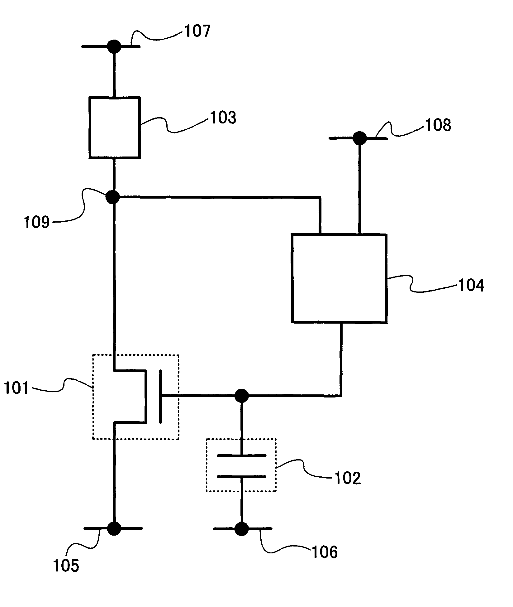
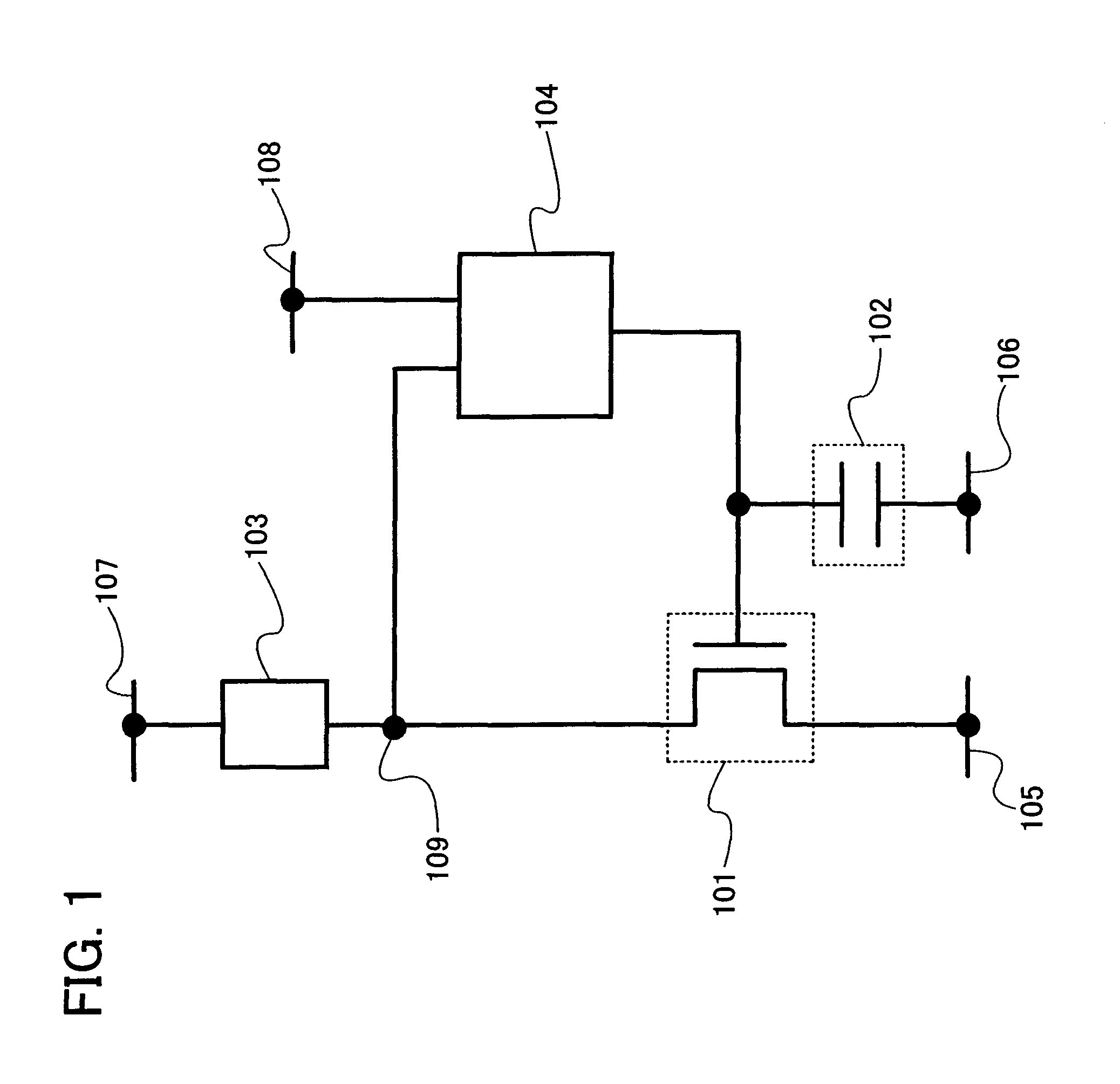
[0136] First, a basic structure of a semiconductor device based on the basic principle of the invention is shown in FIG. 1. The semiconductor device includes a transistor 101, a capacitor 102, a current-voltage converting element 103, and an amplifier circuit 104. It is to be noted that the transistor 101 is an n-channel transistor.

[0137] The transistor 101 has a first terminal (one of a source terminal and a drain terminal) connected to a wire 105, a second ...

embodiment mode 2

[0168] In Embodiment Mode 1, a current flowing through a transistor is controlled by detecting a drain potential of a transistor connected to a current-voltage converting element in series and setting a drain potential of the transistor by an amplifier circuit. In this embodiment mode, description is made of a structure where a current flowing through a transistor is controlled by detecting a drain potential of a transistor connected to a current-voltage converting element in series and setting a source potential of the transistor by an amplifier circuit.

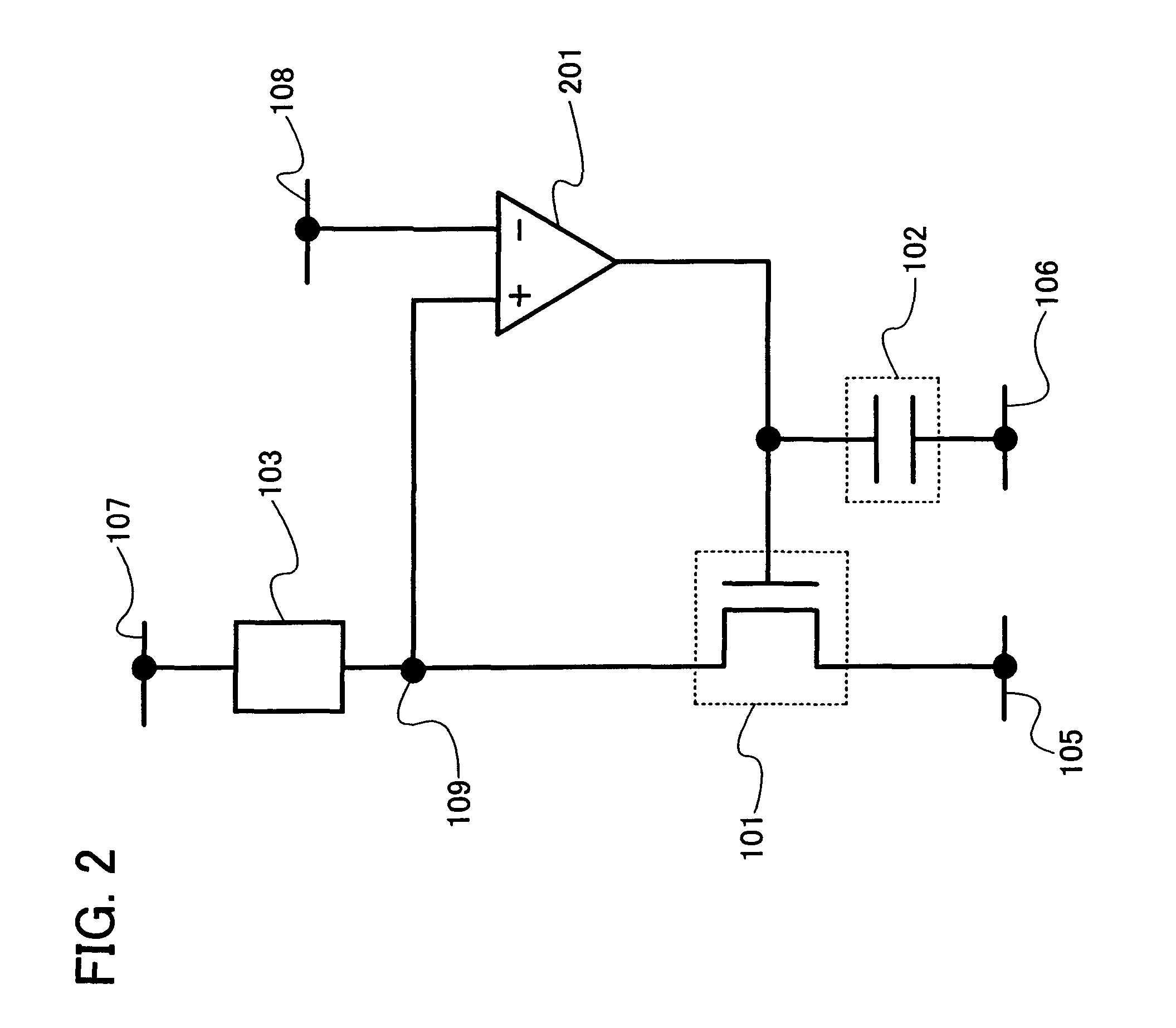
[0169] A semiconductor device shown in FIG. 20 includes a transistor 2001, a capacitor 2002, a current-voltage converting element 2003, and an amplifier circuit 2004. It is to be noted that the transistor 2001 is an n-channel transistor.

[0170] The transistor 2001 has a first terminal (one of a source terminal and a drain terminal) connected to an output terminal of the amplifier circuit 2004, a second terminal (the other of the so...

embodiment mode 3

[0196] In this embodiment mode, description is made of a configuration which can be applied to an amplifier circuit of the semiconductor device described in Embodiment Modes 1 and 2. An operational amplifier or a differential amplifier circuit can be used as the amplifier circuit. Further, a voltage feedback operational amplifier or a current feedback operational amplifier may be used as the amplifier circuit. Alternatively, an operational amplifier additionally provided with various correction circuits such as a phase compensation circuit may be used. It is to be noted that the amplifier circuit described in this embodiment mode can be used in other embodiment modes described later.

[0197] Note that an operational amplifier normally operates so that a potential of a non-inverting input terminal and a potential of an inverting input terminal are equal to each other; however, the potential of the non-inverting input terminal and the potential of the inverting input terminal are not t...


PUM


Abstract

The invention provides a semiconductor device which is capable of decreasing an effect of a variation in characteristics of transistors, supplying a predetermined current even when voltage-current characteristics of a load change, and improving a write speed of a signal sufficiently even when the amount of a signal current is small. In the semiconductor device, a current-voltage converting element and a transistor are connected in series; and an amplifier circuit detects a voltage which is applied when a current flows to the current-voltage converting element, and sets a gate-source voltage of the transistor depending on the voltage. Therefore, since the amplifier circuit has low output impedance, a write speed of a signal can be improved sufficiently even when the amount of a signal current is small.

Description

BACKGROUND OF THE INVENTION [0001] 1. Field of the Invention [0002] The present invention relates to a semiconductor device provided with a function to control a current supplied to a load with a transistor. In particular, the invention relates to a pixel formed of a current-drive light emitting element of which luminance is changed by a current and a display device including a signal line driver circuit for driving a pixel. [0003] 2. Description of the Related Art [0004] As a driving method of a display device using a self-light emitting element typified by an organic light emitting diode (also referred to as an OLED, an organic EL element, an electroluminescence (EL) element, or the like), a simple matrix driving method and an active matrix driving method are known. The former method has a simple structure, but has a problem such as difficulty in realizing a large and high luminance display device. In recent years, an active matrix method has been developed, in which a current flo...

Claims


Application Information

Patent Timeline
Patent Type & Authority Applications(United States)
IPC IPC(8): G09G3/30H05B44/00
CPCG09G3/3241G09G3/325G09G3/3283G09G2320/0252G09G2300/0861G09G2310/027G09G2320/0233G09G2300/0842G11C5/14G11C7/06
Inventor KIMURA, HAJIME
Owner SEMICON ENERGY LAB CO LTD
Why Eureka
Try Eureka