Communication device

a communication device and loopback technology, applied in the direction of digital transmission, pulse automatic control, synchronisation transmitter, etc., can solve the problems of inability to test clock connections and all circuits within the cdr circuit, and inability to detect conditions. to achieve the effect of high speed

Inactive Publication Date: 2007-06-07
NEC ELECTRONICS CORP
View PDF5 Cites 19 Cited by
  • Summary
  • Abstract
  • Description
  • Claims
  • Application Information

AI Technical Summary

Benefits of technology

[0055] The meritorious effects of the present invention are summarized as follows.
[0056] According to the present invention, in the loopback test for a bidirectiona

Problems solved by technology

That is, there is a problem that when a failure such as disconnection in other clock line that does not contribute to the operation has arisen, or when an abnormal condition has been encountered in a circuit other than the some circuits, such a co

Method used


Image

  • Communication device
  • Communication device
  • Communication device

Examples


first embodiment

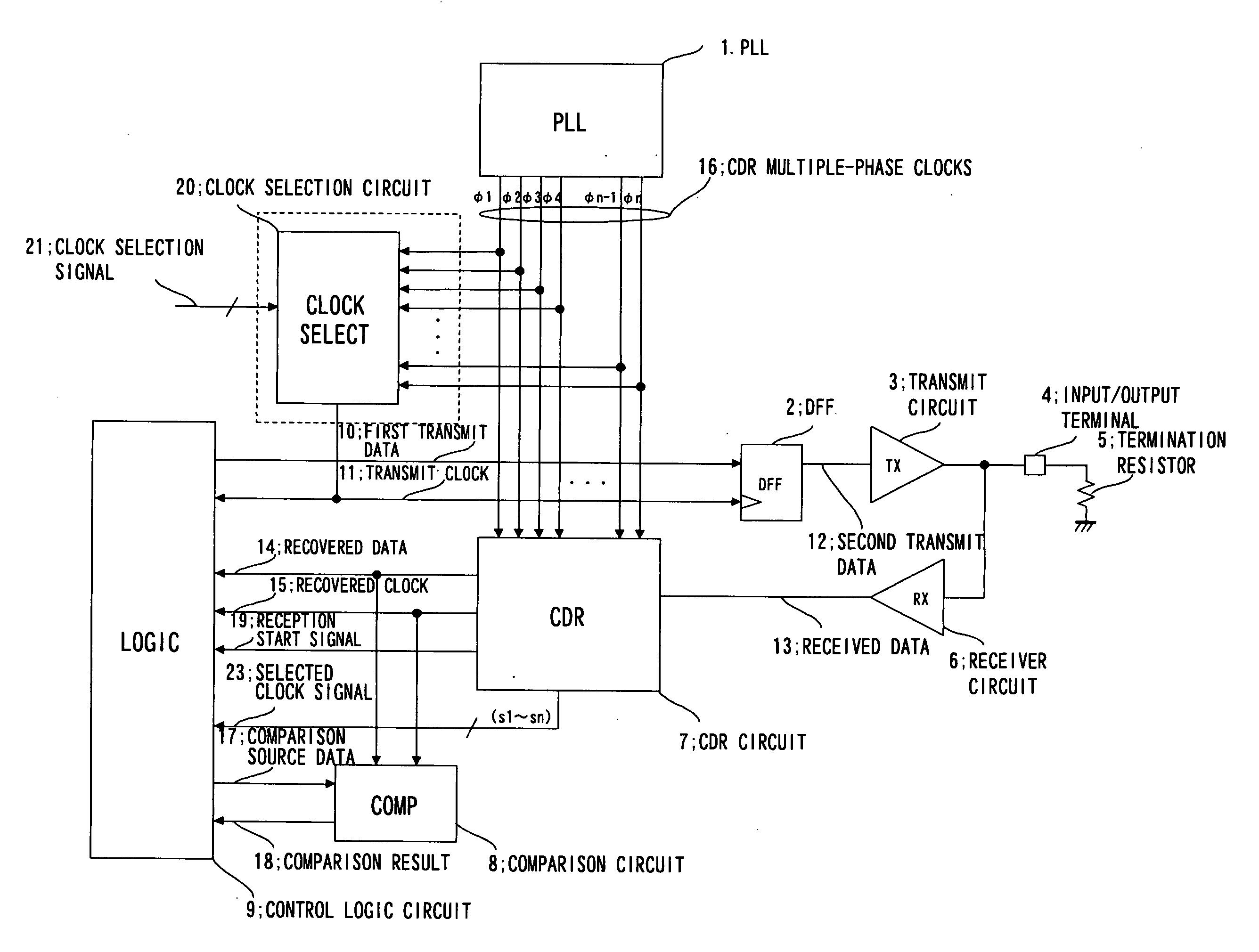
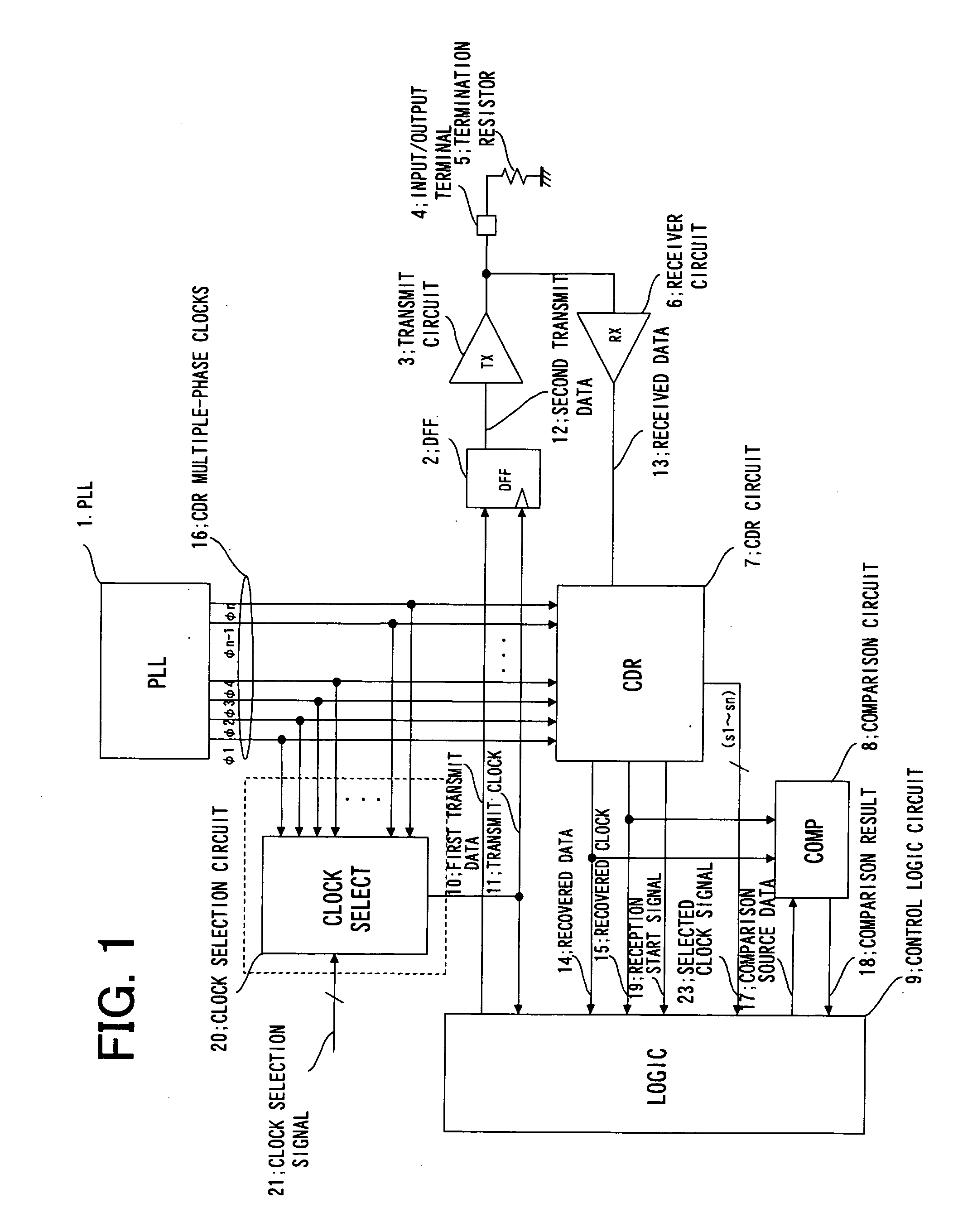
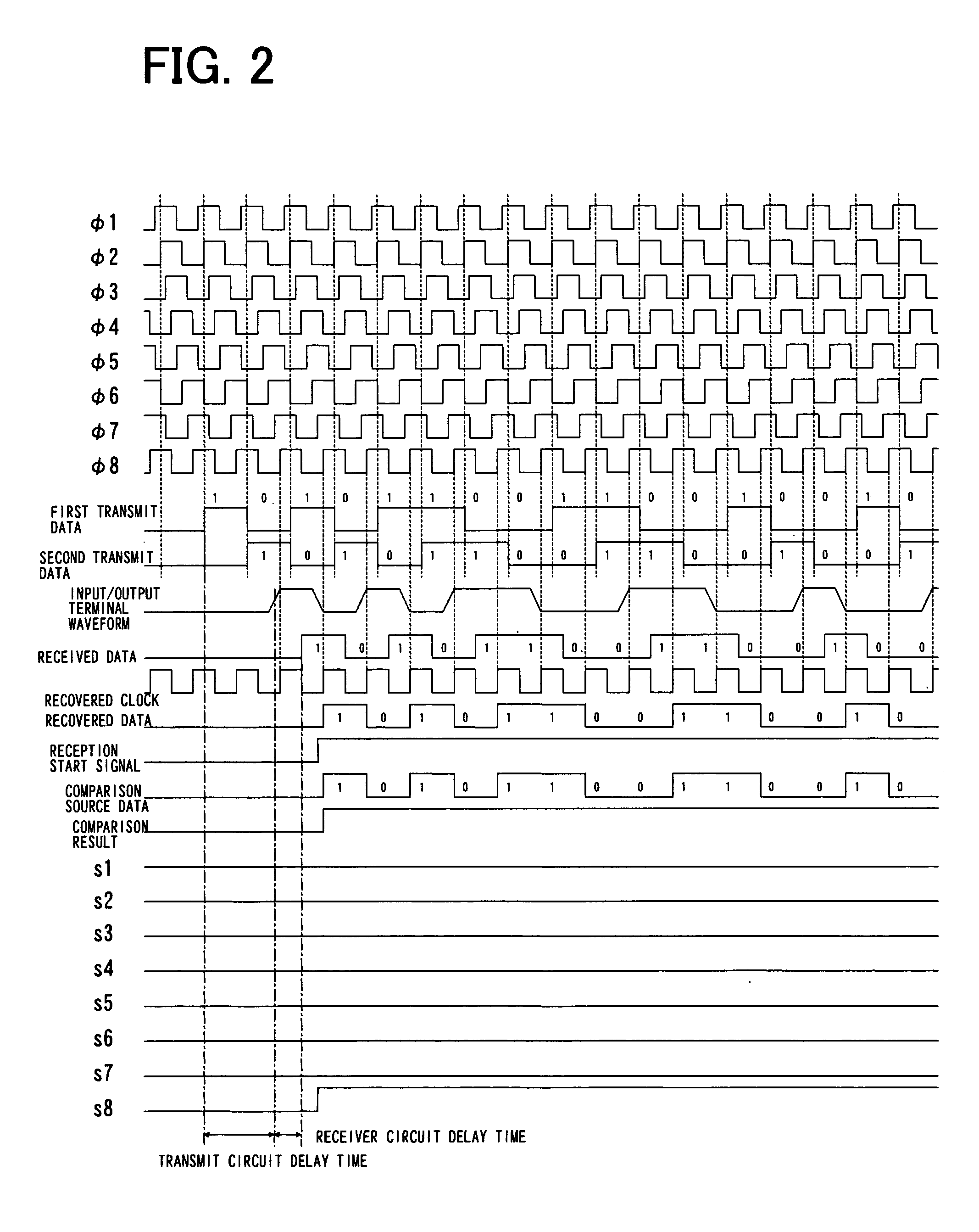
[0073]FIG. 1 is a diagram showing a configuration of the present invention. Referring to FIG. 1, this embodiment includes the PLL circuit 1 (which is an analog PLL), a D-type flip-flop (DFF) 2, a transmit circuit 3 (which is a driver), the input / output terminal 4, a termination resistor 5, the receiver circuit 6 (which is a receiver), the CDR circuit 7, the comparison circuit 8, and a control logic circuit 9 that controls the test. This embodiment further includes the clock selection circuit 20 that receives the multiple-phase clocks 16 output from the PLL 1, selects one of the multiple-phase clocks 16 (of n-phase clocks φ1 to φn in FIG. 1) according to the clock selection signal 21 input from outside, and outputs the selected clock as the transmit clock 11.

[0074] From the PLL 1, the clock signals (referred to as “CDR multiple-phase clocks”) 16 with phases thereof being different to one another are supplied to the CDR circuit 7.

[0075] One of the clock signals having a certain phase...

second embodiment

[0106] In the present invention, shown in FIG. 3, the recovered clock 15 selected by the CDR circuit 7 according to the clock selection signal 21 depends on the transmit circuit delay time (tTx) and the receiver circuit delay time (tRx). Thus, the recovered clock 15 is not uniquely determined. For this reason, when the test is conducted, a state of the second selected clock signal 24 with respect to the clock selection signal 21 needs to be determined in advance. That is, when the clock signal with a certain phase among the multiple-phase clocks 16 is selected at the clock selection circuit 20 as the transmit clock 11, based on the clock selection signal 21, it is necessary to determine in advance which of the second selected clock signal 24 (constituted from the signals t1 to tn) goes HIGH, using measurement or the like.

third embodiment

[0107] On the other hand, in the present invention, as described above, when the fourth-phase clock φ4 of the multiple-phase clocks 16 is selected as the transmit clock 11, selection of the first-phase clock φ1 by the CDR circuit as the recovered clock 15 is managed by the second counter circuit 26, for example.

[0108] In the third embodiment of the present invention, by performing clock input just corresponding to the phase of the clock signal selected by the clock selection circuit 20 before a result of the selection of the recovered clock 15 by the CDR circuit 7 is determined, the test can be always started from the same state.

[0109] According to each of the embodiments described above, clock connections and all circuits within the CDR circuit can be tested at a high speed in an approach of the loopback test. Further, a failure in the clock selection circuit can also be detected.

[0110] Further, according to the third embodiment of the present invention, the test for detection of...


PUM


Abstract

Disclosed is a communication circuit including a clock selection circuit (20) which receives CDR multiple-phase clocks (16) from a PLL (1) to a CDR circuit (7), selects one of the CDR multiple-phase clock signals (16) responsive to a clock selection signal (21), and outputs the selected clock signal. At a time of the loopback test, the clock signal selected by the clock selection circuit (20) is used as a transmit clock (11). Transmit data is looped back from an input/output terminal (4) to a receiver circuit (6). Data from the receiver circuit (6) is supplied to the CDR circuit (7), and comparison between recovered data from the CDR circuit (7) and expected value data is made by a comparison circuit (8), thereby conducting the test. By changing a phase of the transmit clock (11) by the clock selection circuit (20), a delay time (=tTx+tRx) which is a sum of a transmit circuit delay time (tTx) and a receiver circuit delay time (tRx) can be varied.

Description

FIELD OF THE INVENTION [0001] The present invention relates to a loopback test for a communication device. More specifically, the invention relates to a loopback test for a bidirectional, high-speed communication device including a clock and data recovery (CDR) circuit supplied with multiple-phase clocks. BACKGROUND OF THE INVENTION [0002] As a test for a bidirectional, high-speed communication circuit such as the one compliant with USB 2.0 (Universal Serial Bus Specification Revision 2.0), a loopback test has been routinely adopted. In the loopback test, a transmit signal from a transmit unit is directly looped back to a receiver unit, for test, in order to increase efficiency of the test of a transmit / receiver circuit. [0003] Recently, in an advanced miniaturization process of a semiconductor device, a probability of occurrence of a delay failure as well as a function failure of a device that constitutes a circuit becomes higher. Accordingly, the realization of a high-speed test w...

Claims


Application Information

Patent Timeline
IPC IPC(8): H03D3/24H04L69/40
CPCH03L7/06H04L1/243H04L7/0091H04L7/0337
Inventor KAWAKAMI, KENICHI
Owner NEC ELECTRONICS CORP
Why Eureka
Try Eureka