Digital camera

a digital camera and camera body technology, applied in the field of digital cameras, can solve the problems of increasing the volume of the mentioned parts, the number of parts, and achieve the effect of reducing the number of assembly steps and product costs

Inactive Publication Date: 2007-06-07
HON HAI PRECISION IND CO LTD
View PDF1 Cites 49 Cited by
  • Summary
  • Abstract
  • Description
  • Claims
  • Application Information

AI Technical Summary

Benefits of technology

[0008] The main objective of the present invention is to provide a digital camera that can solve the above-mentioned problem. In this digital camera, the optical sensor chip is directly combined with the main circuit board, and the optical sensor chip can be precisely aligned with the optical lens set, and the volume and the number of the parts, the number of assembly steps and product costs can be reduced.

Problems solved by technology

However, the above-mentioned methods increase the volume of the mentioned parts, the number of the parts, the number of assembly steps and product costs.

Method used


Image

  • Digital camera
  • Digital camera
  • Digital camera

Examples


Embodiment Construction

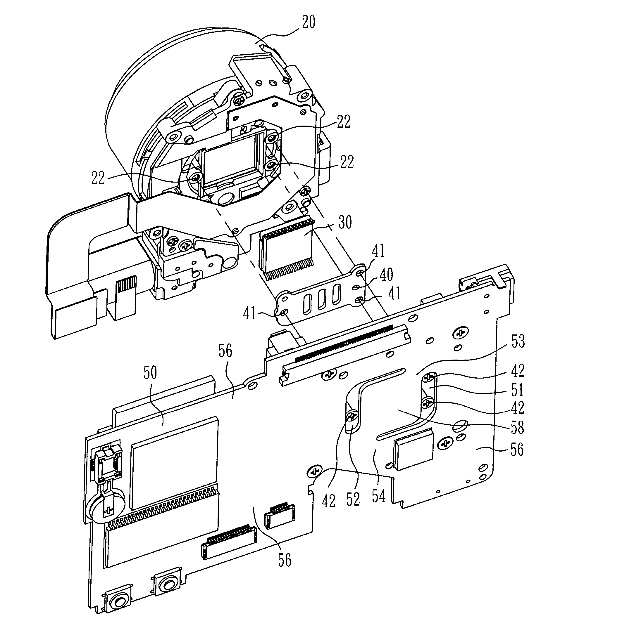
[0020] Please refer to FIG. 3 and FIG. 4. FIG. 3 is a perspective view of a digital camera according to the present invention. FIG. 4 is an exploded view of a digital camera according to the present invention. A digital camera 10 comprises a case 11 and an image capturing control system 12. The image capturing control system 12 comprises an optical lens set 20, an optical sensor chip 30 (such as CCD or CMOS), a mounting seat 40, at least one control button 14, at least one circuit board 50 (the circuit board includes circuitry and electronic units) and a screen 15. Since the basic hardware structure of the digital camera 10 is a very well known technology, it requires no further description.

[0021] A characteristic of the present invention is the combination of the optical lens set 20, the optical sensor chip 30, the mounting seat 40 and the circuit board 50, with particular reference to the mechanism in the circuit board 50.

[0022] Please refer to FIG. 5 to FIG. 7. The circuit boar...


PUM


Abstract

A digital camera has a printed circuit board which comprises a main area and a flexible area. An optical sensor chip (e.g. a CCD) is fixed onto the flexible area. The flexible area has flexible character relative to the main area. Therefore, even if the printed circuit board is stressed, such stress will be almost or completely eliminated in the flexible area, so that the optical sensor chip and an optical lens can be coupled together in a precise manner.

Description

BACKGROUND OF THE INVENTION [0001] 1. Field of the Invention [0002] The present invention relates to digital cameras, and, more particularly, to circuit boards used in digital cameras. [0003] 2. Description of the Related Art [0004] One of the most important things for the manufacturing process of a digital camera is ensuring that the optical lens set and the optical sensor chip (such as charge coupled device, CCD) are perfectly parallel with each other. [0005] Please refer to FIG. 1. FIG. 1 shows a first method of combining an optical lens set and an optical sensor chip together in a prior art prior art digital camera. The optical sensor chip 81 is fixed onto a smaller circuit board 82, and the optical lens set 80 is combined with the optical sensor chip 81. The smaller circuit board 82 is then connected to a primary circuit board (not shown) via a flexible circuit board 83. The primary circuit board is therefore not directly connected to the optical sensor chip 81, and so both dur...

Claims


Application Information

Patent Timeline
Patent Type & Authority Applications(United States)
IPC IPC(8): G03B17/00
CPCG03B17/02H04N5/2253H05K1/0271H05K2201/09063H05K2201/10121H04N23/54
Inventor LU, JIUN-NANHSU, CHIEN-KUOTSAI, CHIH-HSIANG
Owner HON HAI PRECISION IND CO LTD
Why Eureka
Try Eureka