Electronic circuit, method of driving the same, electro-optical device, and electronic apparatus

a technology of electrooptical devices and electronic devices, applied in static indicating devices, instruments, teaching devices, etc., can solve the problems of inability to emitted light by oled devices with correct brightness, and inability to maintain an emission state of current driven devices. to achieve the effect of preventing the power supply voltage from changing

Active Publication Date: 2007-06-07
INTELLECTUAL KEYSTONE TECH LLC
View PDF10 Cites 102 Cited by
  • Summary
  • Abstract
  • Description
  • Claims
  • Application Information

AI Technical Summary

Benefits of technology

[0029] In a preferable aspect of the driving method according to the present invention, an idle time is set between a writing time and a driving time (for example, refer to FIG. 20 or 22). At the idle time, electric connection between the second electrode of the first capacitor and the data line is intercepted and the path through which the driving current is supplied from the power supply line to the light emitting device is intercepted. That is, at the idle time, neither the data voltage is written nor the driving current is supplied to the light emitting device. According to the aspect, it is possible to prevent the writing of the data voltage and the supply of the driving current to the light emitting device from overlapping each other. Therefore, it is possible to prevent the power supply voltage from changing at the writing time so that it is possible to certainly write the data voltage in the electronic circuit. Also, at the idle time between the writing time and the driving time, the second electrode of the first capacitor may float.
[0030] There is provided an electro-optical device including a plurality of scan lines, a plurality of data lines, a plurality of electronic circuits arranged to correspond to the intersections between the plurality of scan lines and the plurality of data lines, a plurality of power supply lines, a scan line driving circuit for driving the plurality of scan lines, and a data line driving circuit for driving the plurality of data lines. The electronic circuits that belong to one group among the plurality of electronic circuits are connected to the plurality of power supply lines. Each of the plurality of electronic circuits includes an electro-optical device, a driving transistor having a first terminal, a second terminal, and a gate terminal and controlling electric connection between the power supply line and the driven device so that the current level of the driving current that flows between the first terminal and the second terminal changes in accordance with the voltage of the gate terminal, a capacitor having a first electrode and a second electrode so that the first electrode is connected to the gate terminal, a first switching device for controlling electric connection between the first terminal of the driving transistor and the power supply line, a second switching device for controlling electric connection between the first terminal or the second terminal of the driving transistor and the gate terminal of the driving transistor, and a third switching device for controlling electric connection between the data line to which the data voltage is supplied and the second terminal of the driving transistor. The same effect as the electronic circuit has is obtained by the electro-optical device. Also, a detailed example of the structure will be described later with reference to FIG. 10.

Problems solved by technology

Also, since the OLED device does not need a back light or reflection light, the OLED device consumes a small amount of power and can be made thin.
Here, a common OLED device is a current driven device that cannot maintain an emission state when current is not supplied since the OLED device does not have a voltage maintaining property unlike the LCD.
However, in the case where one terminal of the capacitor and the source of the driving transistor are connected to the power supply line, when the electric potential of the power supply line changes at the writing time, the voltage maintained in both ends of the capacitor changes so that light cannot be emitted by the OLED device with correct brightness at an emission time.

Method used


Image

  • Electronic circuit, method of driving the same, electro-optical device, and electronic apparatus
  • Electronic circuit, method of driving the same, electro-optical device, and electronic apparatus
  • Electronic circuit, method of driving the same, electro-optical device, and electronic apparatus

Examples


Embodiment Construction

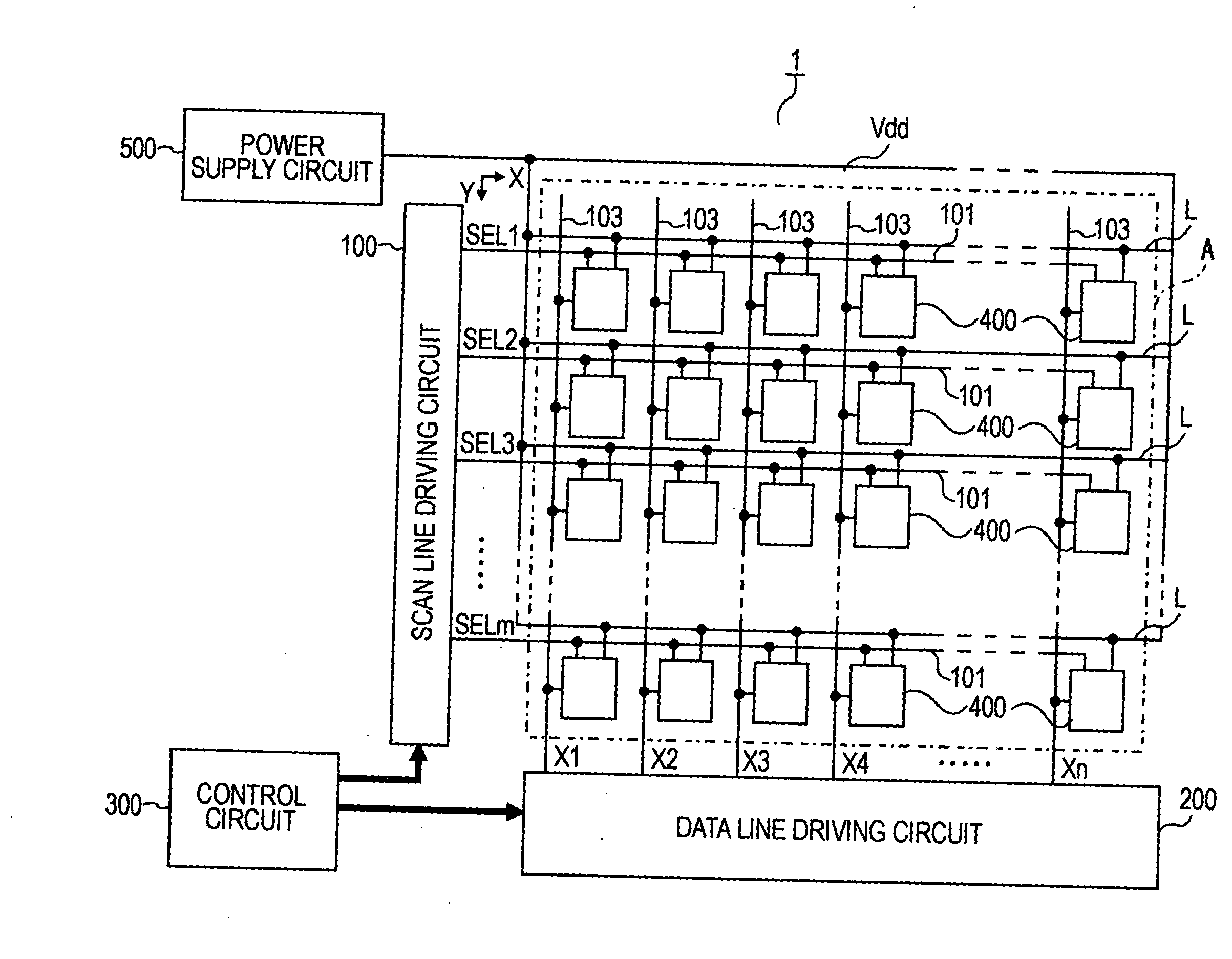
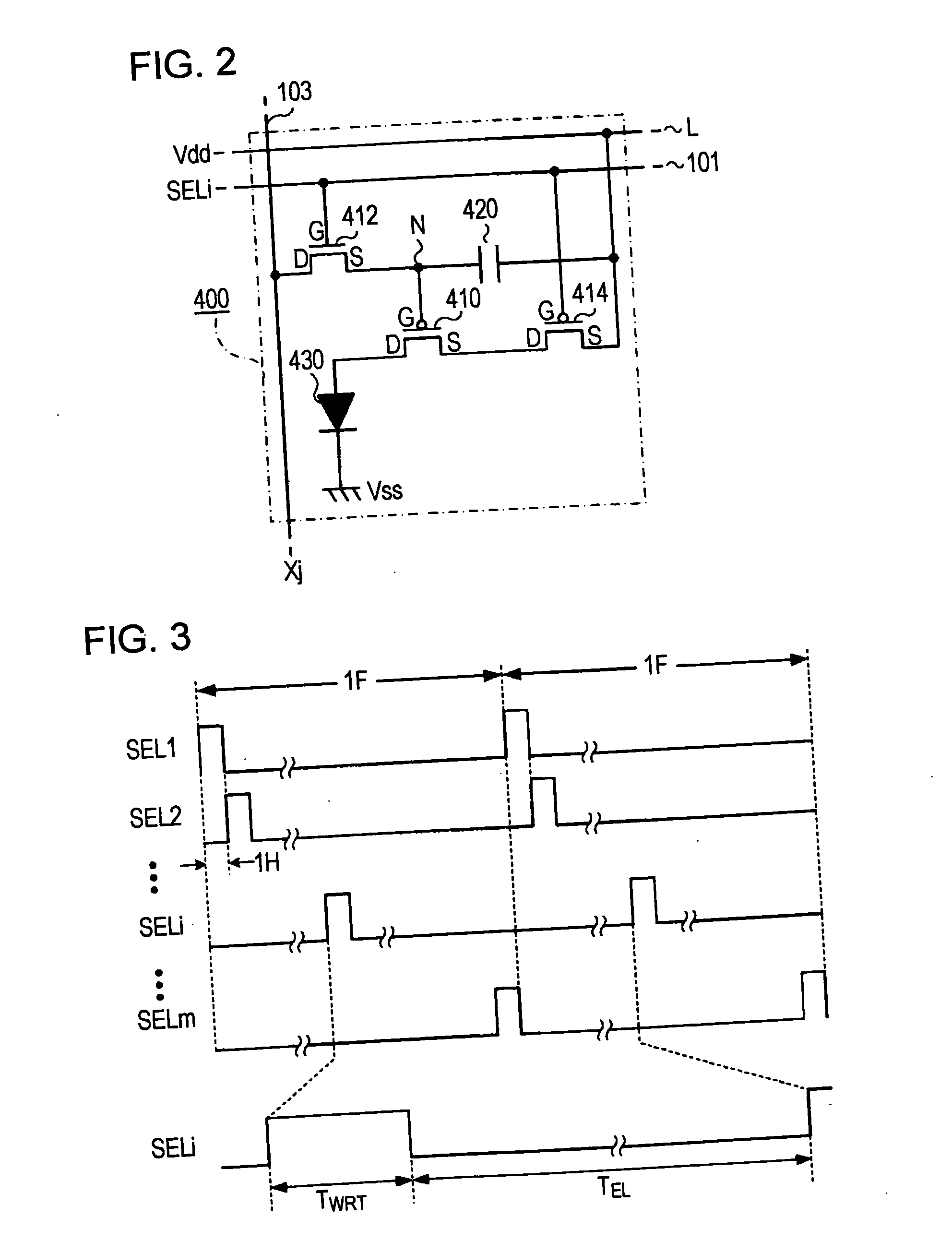
[0061]FIG. 1 is a block diagram illustrating the schematic structure of an electro-optical device including an organic electroluminescence (EL) device (hereinafter, referred to as an OLED device) according to an embodiment of the present invention. FIG. 2 is a circuit diagram of a pixel circuit. As illustrated in FIG. 1, a light emitting device 1 includes a pixel area A, a scan line driving circuit 100, a data line driving circuit 200, a control circuit 300, and a power supply circuit 500. Among them, m scan lines 101 and m power supply lines L that run parallel to the X direction are formed in the pixel area A. Also, n data lines 103 that run parallel to the Y direction that intersects the X direction are formed. One pixel circuit 400 is provided to correspond to each of the intersections between the scan lines 101 and the data lines 103. The pixel circuit 400 includes an OLED device 430. A high electric potential power supply voltage Vdd as a power supply voltage is supplied to th...


PUM


Abstract

At a writing time, a first transistor 412 is turned on so that a data signal Xj is supplied to one end of a capacitor 420. At this time, since a second transistor 414 is turned off, driving current does not flow to an organic light emitting diode (OLED) device 430. A power supply voltage Vdd is supplied to the other end of a capacitor through a power supply line L. However, since the driving current does not flow at the writing time, the power supply voltage Vdd is not reduced by the wiring line resistance of the power supply line L. On the other hand, at an emission time, the first transistor 412 is turned off and the second transistor 414 is turned on. Therefore, the driving current is supplied to the OLED device 430.

Description

[0001] This nonprovisional application claims priority on Japanese Patent Application No. 2005-117873 filed in Japan on Apr. 15, 2005 and Japanese Patent Application No. 2005-120774 filed in Japan on Apr. 19, 2005, the entire contents of which are hereby incorporated by reference. TECHNICAL FIELD [0002] The present invention relates to an electronic circuit used for driving a driven device such as an electro-optical device represented by, for example, a light emitting diode, a method of driving the same, an electro-optical device, and an electronic apparatus. BACKGROUND ART [0003] Recently, an organic light emitting diode (hereinafter, referred to as OLED) device referred to as an organic electroluminescence device or a light emitting polymer device is spotlighted as a next generation light emitting device that replaces a liquid crystal display (LCD). Since the OLED device is of a spontaneous emission type, the OLED device is little dependent on a viewing angle. Also, since the OLED...

Claims


Application Information

Patent Timeline
Patent Type & Authority Applications(United States)
IPC IPC(8): G09B19/00A47B41/00H05B44/00
CPCG09G3/3233G09G2300/0465G09G2300/0814Y02B20/36G09G2300/0876G09G2320/043H05B33/0896G09G2300/0861H05B45/60Y02B20/30H01L2027/11879G09G3/3266G09G2310/08
Inventor MIYAZAWA, TAKASHI
Owner INTELLECTUAL KEYSTONE TECH LLC
Why Eureka
Try Eureka