Testable design methodology for clock domain crossing

a clock domain and design methodology technology, applied in the field of testing methodology, can solve the problems of difficult debugging of single domain test structures, inability to debug designs in single domain, and difficulty in debugging and testing synchronizing logic circuits

Inactive Publication Date: 2007-06-07
AVAGO TECH WIRELESS IP SINGAPORE PTE
View PDF3 Cites 12 Cited by
  • Summary
  • Abstract
  • Description
  • Claims
  • Application Information

AI Technical Summary

Problems solved by technology

For complex silicon chips, silicon debugging is one of the more difficult of system designs, due to inherent lack of visibility into the design state.
For logic signals that traverse clock domains, single domain test structures may not allow for the debugging of designs and functionality of synchronizing circuits that are used to control the signal traversal from one clock domain to another clock domain.
Since multiple layers of logic complexity may be designed on top of some synchronizing circuits, debugging and testing of synchronizing logic circuitry is difficult to achieve when debug procedures are limited to looking at signals in a single clock domain.
Furthermore, synchronization logic circuits are generally not testable directly through software.
During functional testing, it is not possible to determine directly as a part of the functional test, whether a logic state traversal occurs properly across the clock domains bridged by the synchronizing circuit.
However, such scan techniques do not offer a fine enough granularity at a logic level of the synchronizing circuit to determine if exactly one traversal occurred consistently.

Method used


Image

  • Testable design methodology for clock domain crossing
  • Testable design methodology for clock domain crossing
  • Testable design methodology for clock domain crossing

Examples


Embodiment Construction

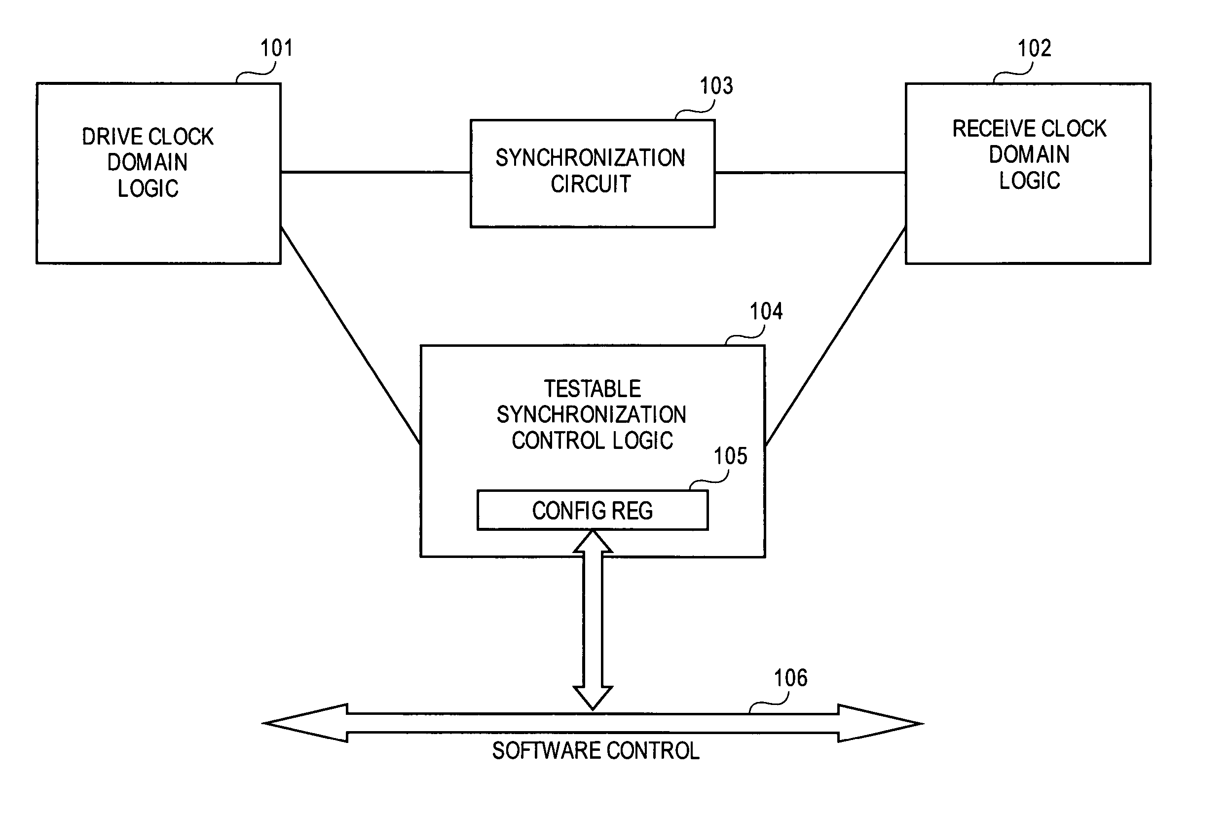
[0013] The embodiments of the present invention may be practiced in a variety of settings that implement multiple clock domains. The examples below describe embodiments of the invention in which at least two different clock domains are resident on an integrated circuit device and bridged by a synchronization circuit. However, other embodiments may be employed in which other circuits are used to transfer a signal across clock domains.

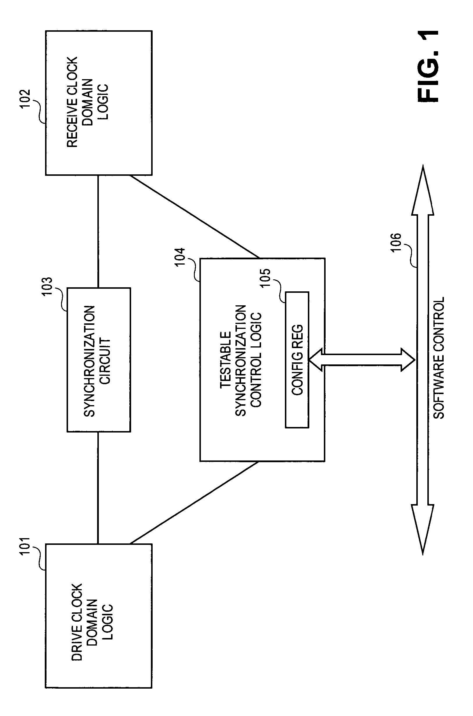
[0014] Referring to FIG. 1, an example circuit 100 is shown. Circuit 100 is part of an integrated circuit (IC), in which the IC includes various other circuitry (not shown) as well. The exemplary circuit 100 is shown having two clock domains. The IC may have more than two clock domains, but only two are shown for illustrative purpose in FIG. 1. A drive clock domain logic 101 operates in a first clock domain and a receive clock domain logic 102 operates in a second clock domain. A synchronization circuit 103 is coupled to both clock domain logics 101, 10...


PUM


Abstract

A design methodology to debug synchronization of a signal crossing clock domains. A testable synchronization control logic utilizes a programmable register to set parameters to test signals traversing from one clock domain to another clock domain across a synchronization circuit. The register is programmed with a latency value that corresponds to a correct synchronization timing for the clock domain crossing. Other bit entries in the register provide setting of other debug parameters and indications of monitored results.

Description

BACKGROUND OF THE INVENTION [0001] 1. Technical Field of the Invention [0002] The embodiments of the invention relate to testing methodology and, more particularly, to test signals crossing clock domains. [0003] 2. Description of Related Art [0004] When an integrated circuit (IC) is manufactured, the IC chip undergoes a variety of testing to validate the design of the chip. For complex silicon chips, silicon debugging is one of the more difficult of system designs, due to inherent lack of visibility into the design state. In order to facilitate the performing of the debug procedures, various test and debug structures are designed into the IC. These test and debug structures are then accessed during a debug phase when testing the IC. [0005] Although many such test and debug structures may be present in a chip, most are designed to address debugging within a single clock domain. For logic signals that traverse clock domains, single domain test structures may not allow for the debuggin...

Claims


Application Information

Patent Timeline
Patent Type & Authority Applications(United States)
IPC IPC(8): G01R31/28G06F11/00
CPCG01R31/31725G01R31/318594
Inventor JAMKHANDI, PIYUSH
Owner AVAGO TECH WIRELESS IP SINGAPORE PTE
Why Eureka
Try Eureka