Triple-well low-voltage-triggered ESD protection device

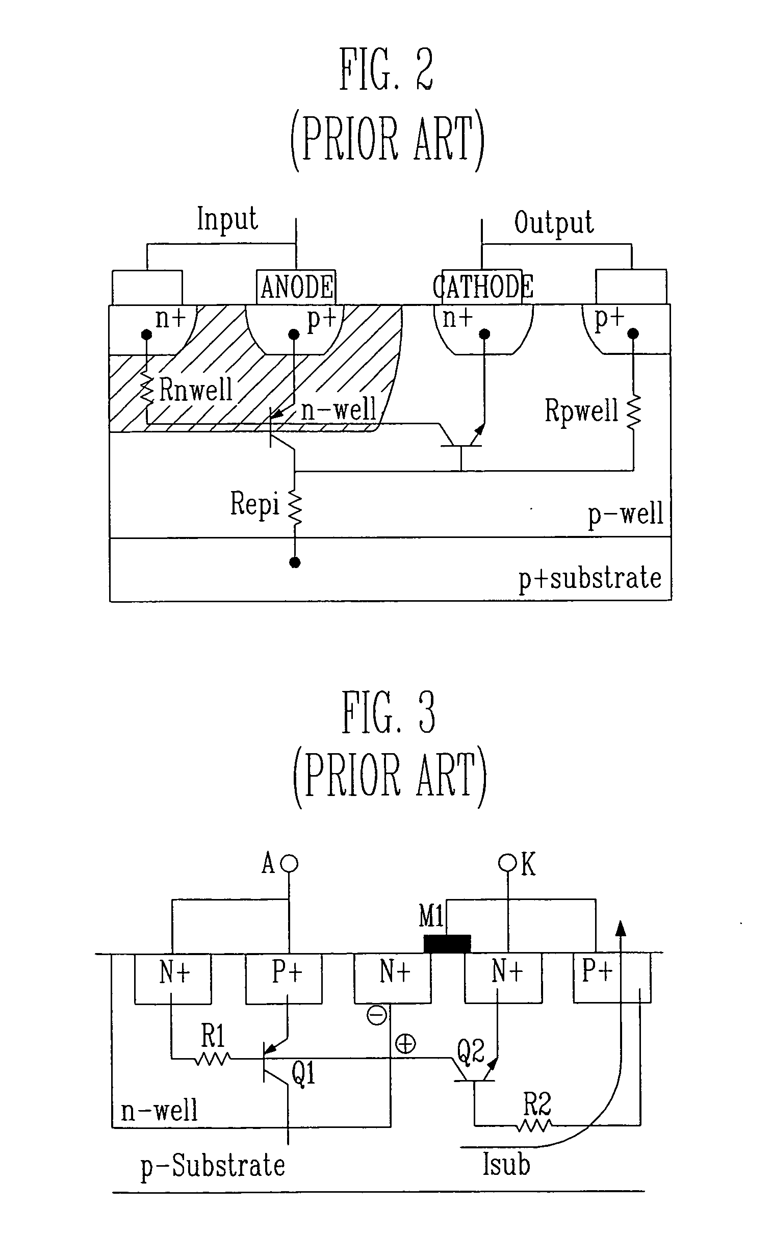
a protection device and three-well technology, applied in semiconductor devices, transistors, electrical equipment, etc., can solve the problems of esd-related device breakdown, affecting the operation of low-voltage vdsm-level circuits, and the trigger voltage is still too high to apply lvtscr to high-speed, low-voltage circuits. , the effect of reducing the trigger voltag

Inactive Publication Date: 2007-06-14
ELECTRONICS & TELECOMM RES INST
View PDF11 Cites 24 Cited by
  • Summary
  • Abstract
  • Description
  • Claims
  • Application Information

AI Technical Summary

Benefits of technology

[0016] The invention improves upon the high trigger voltage of a conventional ESD protection device, enabling faster response to an ESD pulse by connecting an RC network there to the ESD protection device, and thus is applicable to a high-speed, low-voltage integrated circuit designed and fabricated by VSDM pro

Problems solved by technology

ESD, the abrupt discharge of static electricity generated during the production and use of electrical devices and components, is becoming an important concern in the design of integrated circuits because it can cause the breakdown of an integrated circuit internal device and metal interconnections.
Consequently, device breakdown caused by ESD is becoming a more serious problem.
However, since the common SCR has a very high trigger voltage of about 30V, the gate oxide layer of a MOS

Method used


Image

  • Triple-well low-voltage-triggered ESD protection device
  • Triple-well low-voltage-triggered ESD protection device
  • Triple-well low-voltage-triggered ESD protection device

Examples


Embodiment Construction

[0023] Hereinafter, exemplary embodiments according to the invention will be described in detail with reference to the accompanying drawings. The following exemplary embodiments are described so that this disclosure is comprehensive and enabling of practice of the invention by those of ordinary skill in the art. The invention may, however, be embodied in different forms and should not be construed as limited to the exemplary embodiments set forth herein.

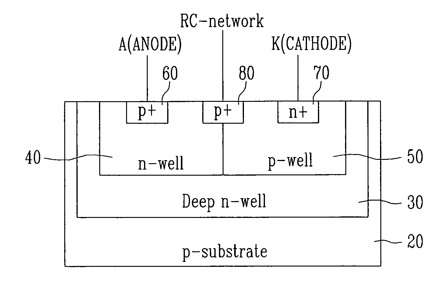
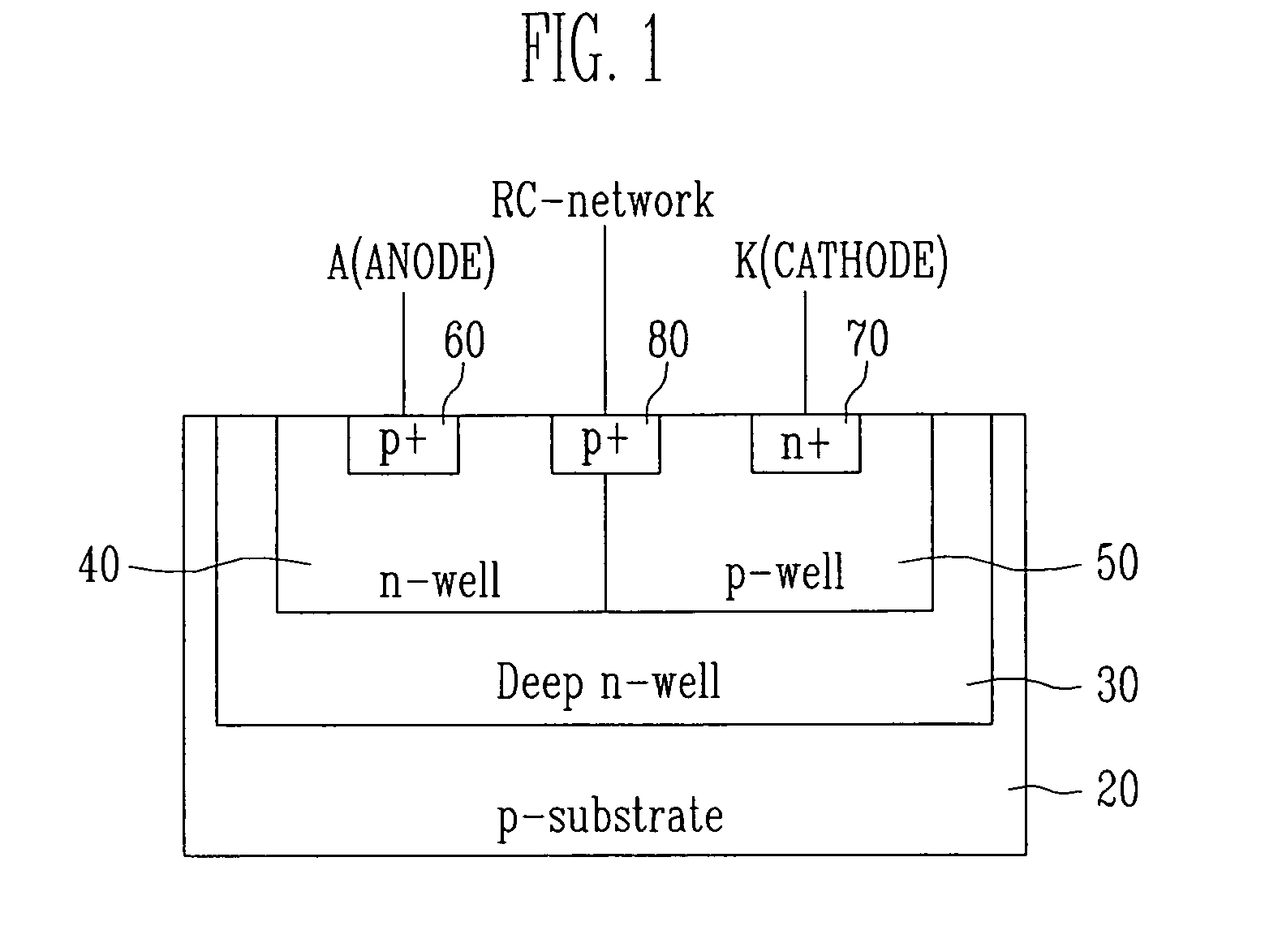
[0024] In the first exemplary embodiment of the invention, key technical aspects of embodiment of a triple-well low-voltage-triggered ESD protection device are as follows:

[0025] First, a method of embodying a silicon controlled rectifier (SCR) for improved electrostatic discharge (ESD) protection of a CMOS chip in a very deep sub-micron (VDSM) process is presented;

[0026] Second, a technique of forming a deep well is presented to form a triple-well structure; and

[0027] Third, a technique of forming a p+ having a high doping concen...


PUM


Abstract

An ESD protection device with a silicon controlled rectifier (SCR) structure which is applied to a nano-device-based high-speed I/O interface circuit and semiconductor substrate operated by a low power voltage. The triple-well low-voltage-triggered ESD protection device includes: a deep n-type well formed on a p-type substrate; n- and p-type wells formed to be mutually connected in the deep n-type well; and a bias application region for applying a direct bias voltage to the p-type well.

Description

CROSS-REFERENCE TO RELATED APPLICATION [0001] This application claims priority to and the benefit of Korean Patent Application Nos. 2005-119535, filed Dec. 8 2005, and 2006-76773, filed Aug. 14, 2006, the disclosures of which are incorporated herein by reference in their entirety. BACKGROUND [0002] 1. Field of the Invention [0003] The present invention relates to an electrostatic discharge (ESD) protection device for protecting an internal circuit from shock such as external static electric shock, etc. in semiconductor device technology, and more particularly, to an ESD protection device with a triple-well structure improved the shortcomings of a common silicon controlled rectifier (SCR) and a low-voltage-triggered SCR (LVTSCR) employed in a conventional ESD protection circuit. [0004] 2. Discussion of Related Art [0005] ESD, the abrupt discharge of static electricity generated during the production and use of electrical devices and components, is becoming an important concern in the...

Claims


Application Information

Patent Timeline
IPC IPC(8): H02H9/00
CPCH01L27/0262H01L29/7436
Inventor KIM, KWI DONGKWON, CHONG KIKIM, JONG DAEKOO, YOUNG SEO
Owner ELECTRONICS & TELECOMM RES INST
Why Eureka
Try Eureka