Structure and method for thin single or multichip semiconductor QFN packages

a technology of semiconductor qfn and structure, applied in semiconductor devices, semiconductor/solid-state device details, electrical devices, etc., can solve the problems of increasing the difficulty of increasing the difficulty of finding satisfactory solutions for diverse requirements, and increasing the difficulty of maintaining mold compound adhesion to the leadframe, etc., to achieve the effect of easy control

Inactive Publication Date: 2007-06-14
TEXAS INSTR INC
View PDF20 Cites 17 Cited by
  • Summary
  • Abstract
  • Description
  • Claims
  • Application Information

AI Technical Summary

Benefits of technology

[0013] It is an advantage that the grinding technique does not require specific powders, rinsing or cleaning, and the grinding rate is equal for the involved metals, polymers, and semiconductors. The employed technique is easy to control, an advantage for fabricating ultra-thin packages.

Problems solved by technology

For electrical and thermal reasons, copper has been the favorite starting material; however, the copper price has recently been climbing sharply.
In recent years, a number of technical and market trends have made it more and more difficult to find satisfactory solutions for the diverse requirements.
Then, the requirement to use lead-free solders pushes the reflow temperature range into the neighborhood of about 260° C., making it more difficult to maintain mold compound adhesion to the leadframes.
ICs are becoming faster; consequently, they dissipate more thermal energy, which needs to be removed to maintain optimum operating temperatures.

Method used


Image

  • Structure and method for thin single or multichip semiconductor QFN packages
  • Structure and method for thin single or multichip semiconductor QFN packages
  • Structure and method for thin single or multichip semiconductor QFN packages

Examples


Embodiment Construction

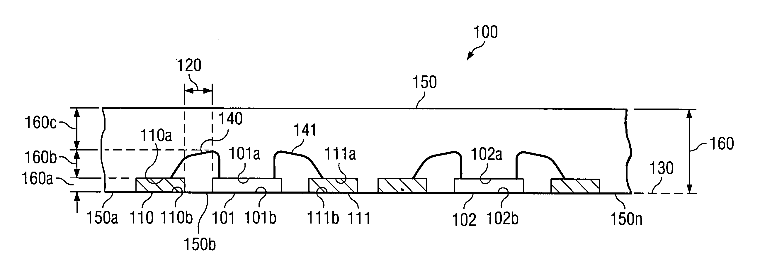
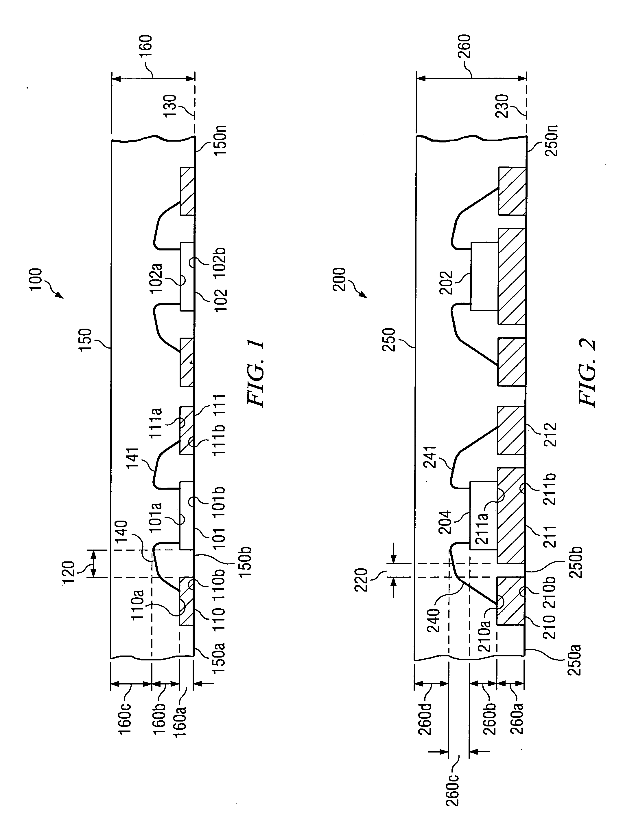
[0028]FIGS. 1 and 2 are schematic cross sections of embodiments of the present invention. FIG. 1 shows a multichip device of the QFN (Quad Flat No-lead) or SON (Small Outline No-lead) family, generally designated 100, with two similar chips 101 and 102. It should be stressed, however, that the considerations about device 100 are equally valid, when device 100 contains only a single chip, or more than two chips; also, the considerations are equally valid, when the chips of a multichip device are dissimilar or belonging to different product families.

[0029] Using chip 101 as an example, FIG. 1 illustrates chip 101 having an active surface 101a and a passive surface 101b. The active surface 101a includes contact pads suitable for affixing conductive connectors. In analogy, chip 102 has an active surface 102a with contact pads, and a passive surface 102b.

[0030] Device 100 in FIG. 1 further has a plurality of metal segments 110, 111, etc., which are separated from chips 101 and 102 by g...


PUM


Abstract

A semiconductor device (100) has one or more semiconductor chips (110) with active and passive surfaces, wherein the active surfaces include contact pads. The device further has a plurality of metal segments (111) separated from the chip by gaps (120); the segments have first and second surfaces, wherein the second surfaces (111b) are coplanar (130) with the passive chip surface (101b). Conductive connectors span from the chip contact pads to the respective first segment surface. Polymeric encapsulation compound (150) covers the active chip surface, the connectors, and the first segment surfaces, and are filling the gaps so that the compound forms surfaces coplanar (130) with the passive chip surface and the second segment surfaces. In this structure, the device thickness may be only about 250 μm. Reflow metals may be on the passive chip surface and the second segment surfaces.

Description

FIELD OF THE INVENTION [0001] The present invention is related in general to the field of semiconductor devices and processes, and more specifically to structure and method of thin single or multichip semiconductor QFN devices. DESCRIPTION OF THE RELATED ART [0002] Leadframes for semiconductor devices provide a stable support pad for firmly positioning the semiconductor chip, usually an integrated circuit (IC) chip, within a package. It has been common practice to manufacture single piece leadframes from thin (about 120 to 250 μm) sheets of metal. For electrical and thermal reasons, copper has been the favorite starting material; however, the copper price has recently been climbing sharply. [0003] In addition to the chip pad, the leadframe offers a plurality of conductive segments to bring various electrical conductors into close proximity of the chip. The remaining gaps between the segments and the contact pads on the chip surface are bridged by connectors, typically thin metal wir...

Claims


Application Information

Patent Timeline
Patent Type & Authority Applications(United States)
IPC IPC(8): H01L23/495H01L21/00
CPCH01L21/4832H01L21/561H01L21/568H01L21/6835H01L23/3107H01L24/45H01L24/97H01L2221/68377H01L2224/45144H01L2224/48091H01L2224/48247H01L2224/97H01L2924/01013H01L2924/01014H01L2924/01029H01L2924/01032H01L2924/0105H01L2924/01079H01L2924/01082H01L2924/01322H01L2924/12044H01L2924/14H01L2924/18165H01L2924/00014H01L2224/85H01L24/48H01L2924/01005H01L2924/01006H01L2924/01023H01L2924/01033H01L2924/01028H01L2924/10253H01L2924/00H01L2924/181H01L2924/00012
Inventor MASUMOTO, MUTSUMI
Owner TEXAS INSTR INC
Why Eureka
Try Eureka