Printed circuit board having embedded electronic components and manufacturing method thereof

a technology of electronic components and printed circuit boards, which is applied in the direction of printed circuit aspects, printed circuit non-printed electric components association, electrical apparatus construction details, etc., can solve the fundamental limit affecting yield, and raising the cost of manufacture. achieve the effect of increasing the number of embedded electronic components, improving heat release, and maintaining strength

Inactive Publication Date: 2007-06-14
SAMSUNG ELECTRO MECHANICS CO LTD
View PDF4 Cites 35 Cited by
  • Summary
  • Abstract
  • Description
  • Claims
  • Application Information

AI Technical Summary

Benefits of technology

The present invention provides a printed circuit board with embedded components that are thinner than traditional circuit boards but still maintain strength. Additionally, the invention improves heat release, which allows for more embedded electronic components.

Problems solved by technology

The patent text discusses the challenges in developing printed circuit boards with embedded electronic components. These boards have advantages such as multi-functionality and miniaturization, but they also face problems like heat release and delamination. The current process of embedding electronic components also has limitations in terms of bending strength and the number of components embedded. The technical problem addressed in the patent is to provide a technology that strengthens thin printed circuit boards and improves heat-releasing properties, as well as to overcome the limitations of the current embedding process.

Method used


Image

  • Printed circuit board having embedded electronic components and manufacturing method thereof
  • Printed circuit board having embedded electronic components and manufacturing method thereof
  • Printed circuit board having embedded electronic components and manufacturing method thereof

Examples


Embodiment Construction

[0037] Certain embodiments of the present invention will be described below in more detail with reference to the accompanying drawings. In the description with reference to the accompanying drawings, those components are rendered the same reference number that are the same or are in correspondence regardless of the figure number, and redundant explanations are omitted.

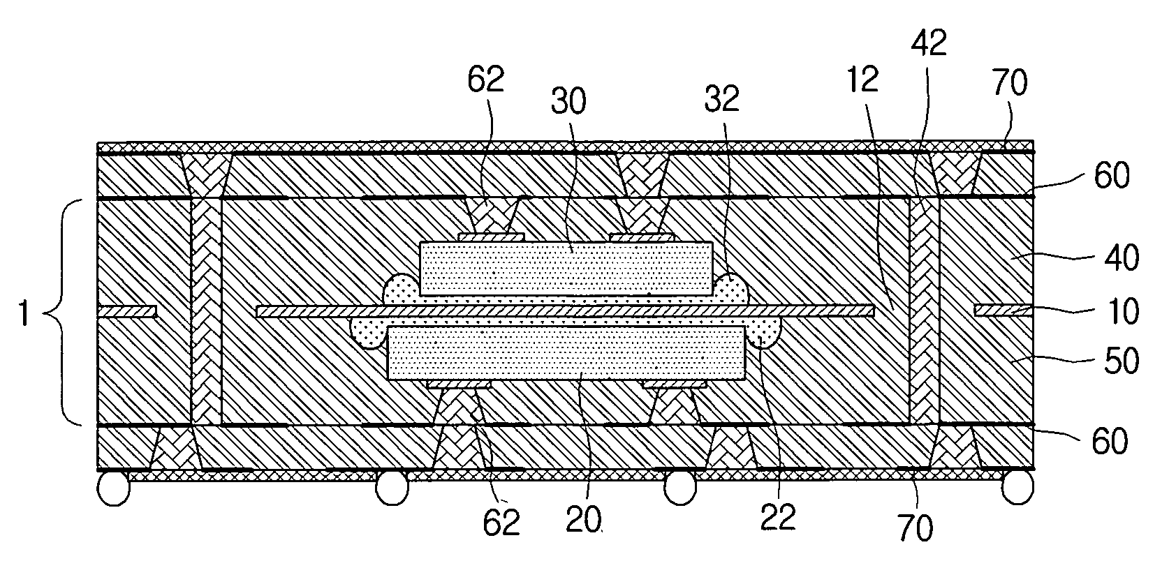
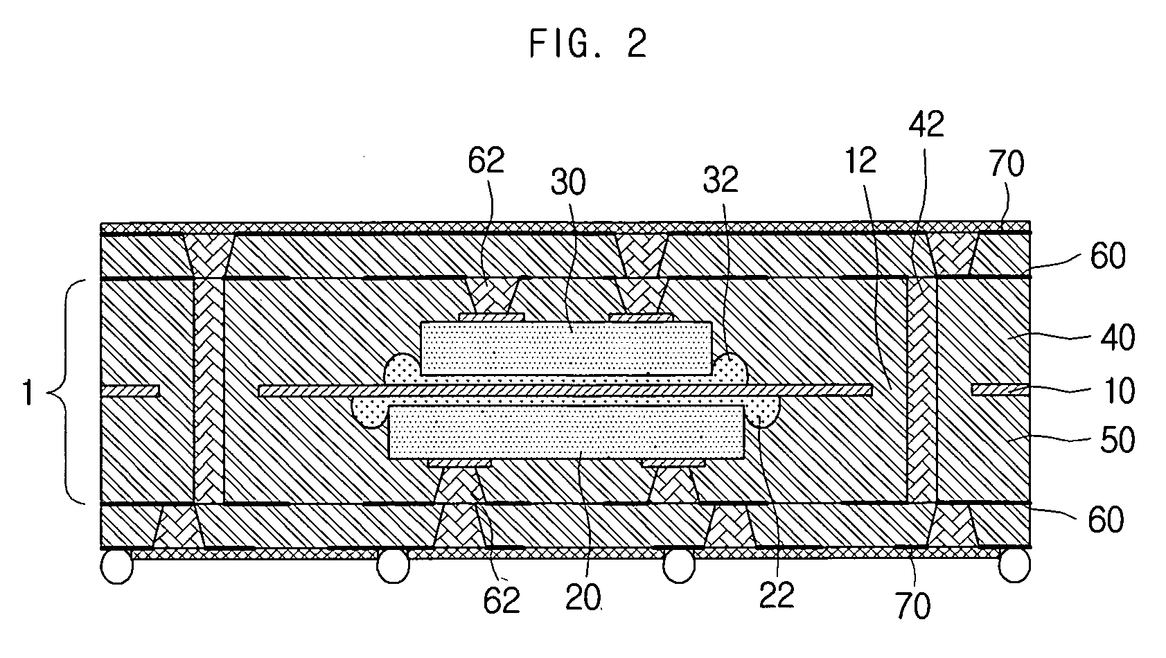
[0038]FIG. 2 is a cross-sectional view of a printed circuit board having embedded electronic components based on a first disclosed embodiment of the present invention. In FIG. 2 are illustrated a core substrate 1, a core sheet 10, core holes 12, a first electronic component 20, a second electronic component 30, chip adhesive 22, 32, a first insulation layer 40, IVH's 42, a second insulation layer 50, circuit patterns 60, BVH's 62, and outer layer circuits 70.

[0039] A feature of the present invention is the structure of the core substrate 1, in which several electronic components are embedded while maintaining symmetr...


PUM

PropertyMeasurementUnit
Timeaaaaaaaaaa
Sizeaaaaaaaaaa
Shapeaaaaaaaaaa

Abstract

A printed circuit board having embedded electronic components and a manufacturing method thereof are disclosed. With the printed circuit board having embedded electronic components, including a core sheet, a first electronic component mounted on one side of the core sheet, a second electronic component mounted on the other side of the core sheet and overlapping the first electronic component, a first insulation layer stacked on one side of the core sheet and covering the first electronic component, a second insulation layer stacked on the other side of the core sheet and covering the second electronic component, and a circuit pattern formed on the surface of the first insulation layer or the second insulation layer, the density of the printed circuit board having embedded components is improved, as a plurality of electronic components are embedded simultaneously, and when a thin CCL substrate or a metal substrate is used as the core, a metal substrate in particular, the heat-releasing property and mechanical strength are improved, including increased bending strength in a thermal-stress environment, as electronic components are mounted on both sides of the core sheet.

Description


Claims


Application Information

Patent Timeline
Owner SAMSUNG ELECTRO MECHANICS CO LTD
Why Eureka
Try Eureka