
Devices and methods for inspecting optical elements with a view to contamination

a technology of optical elements and inspection methods, applied in the field of inspection of optical elements with a view to contamination, can solve the problems of contaminating the surface of some of their optical elements, affecting the use of instruments, and expensive materials compared to normal float glass for display purposes, and the known methods for measuring scattered light in an optical system cannot unequivocally locate the source of scattered light. , to achieve the effect of preventing the saturation of detectors

Inactive Publication Date: 2007-06-14
CARL ZEISS SMT GMBH
View PDF6 Cites 38 Cited by
  • Summary
  • Abstract
  • Description
  • Claims
  • Application Information

AI Technical Summary

Benefits of technology

The invention provides an examination system that can locate contamination on optical elements in optical systems without needing to remove them from the system. The system uses a spatially resolving detector and magnifying imaging optics to precisely locate contamination on the surface of the optical element. The system can also be used in microlithography apparatus or projection illumination apparatus for microlithography. The invention also provides a method for removing contamination from the surface of an optical element and a method for determining the thickness of a contamination layer on the surface of an optical element. The movement mechanism of the system allows for scanning the surface of the optical element to examine it more precisely. The invention is advantageous for identifying and locating contamination on optical elements in optical systems.

Problems solved by technology

Optical devices, in particular systems in which short-wave radiation is used, such as e.g. projection illumination apparatus for lithography optics, or systems for inspecting photomasks and wafers, as well as laser systems e.g. for laser machining apparatus, in particluar UV laser systems and systems for guiding their beams, are associated with the danger that the surfaces of some of their optical elements become contaminated as a result of the atmosphere surrounding them.
Such materials are expensive compared to normal float glass for display purposes.
However, the known methods for measuring scattered light in an optical system cannot unequivocally locate the source of the scattered light, wherein e.g. the depositing of material on at least one optical surface of the optical system is considered to be one possible source.

Method used


Image

  • Devices and methods for inspecting optical elements with a view to contamination
  • Devices and methods for inspecting optical elements with a view to contamination
  • Devices and methods for inspecting optical elements with a view to contamination

Examples


Embodiment Construction

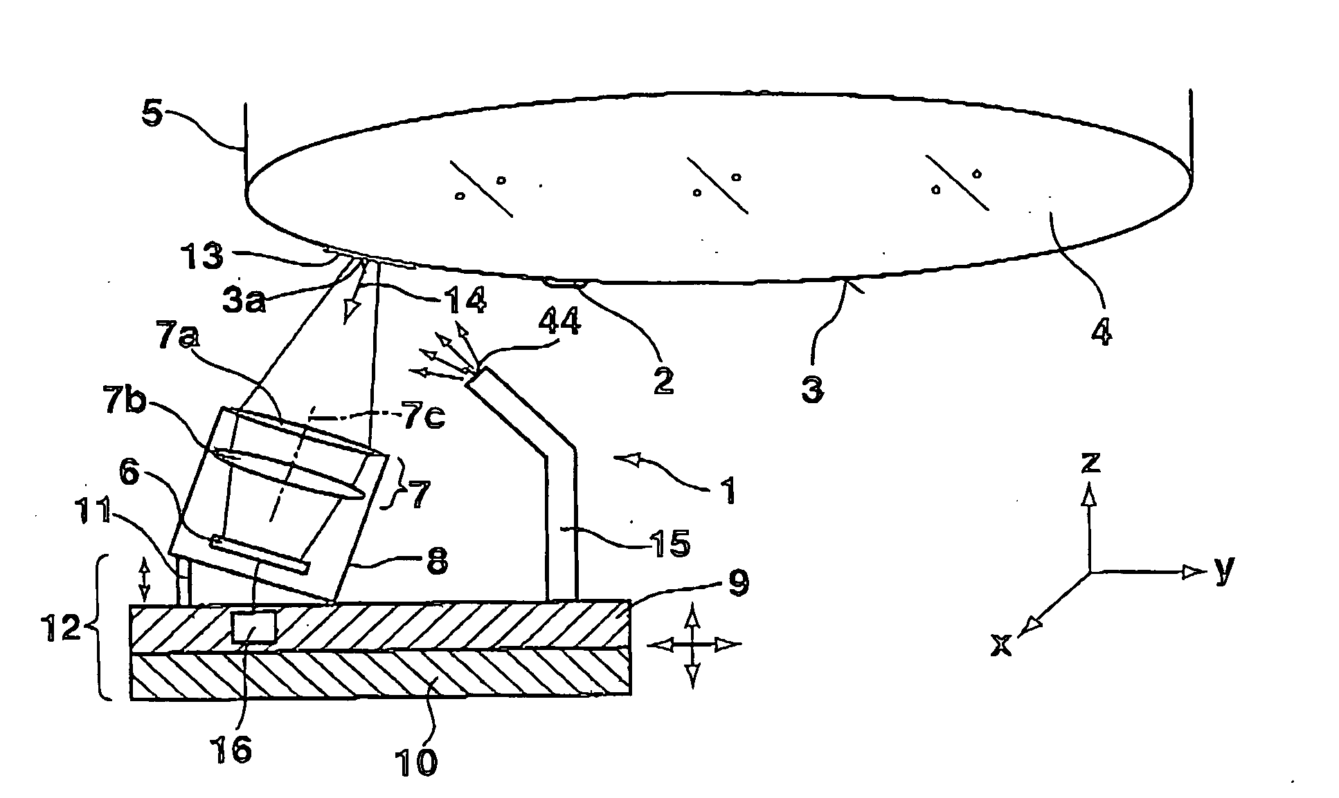
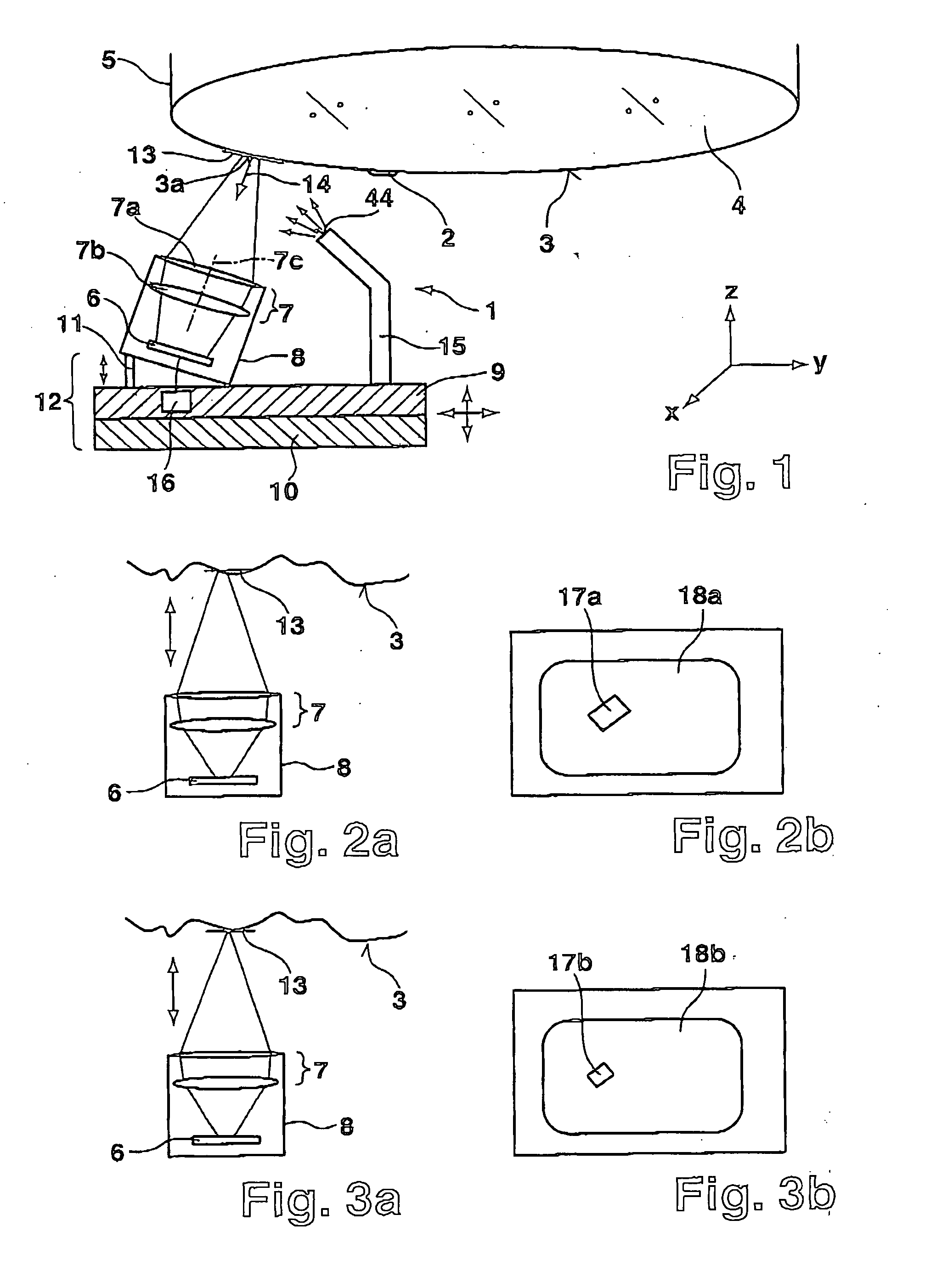
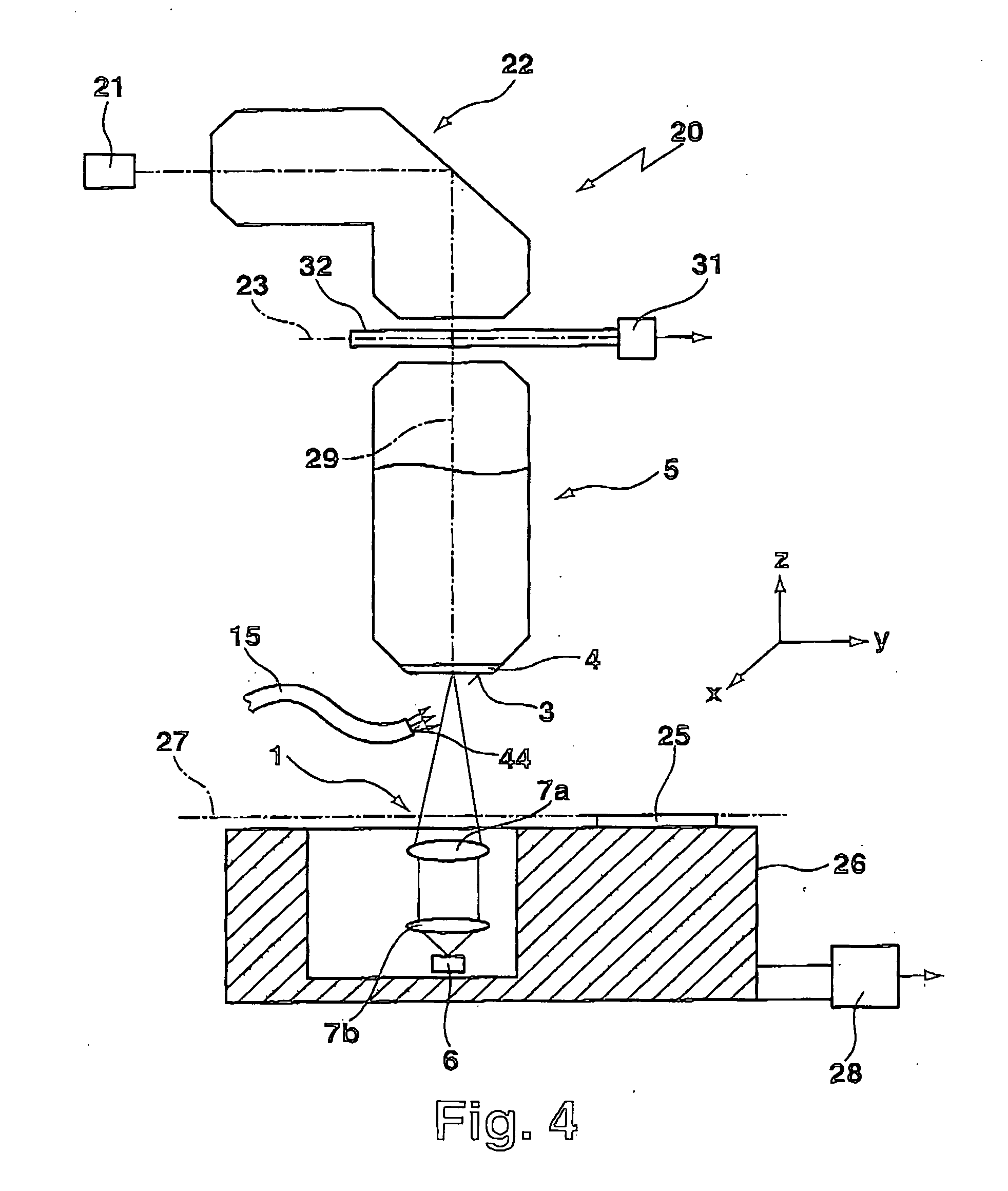
[0102]FIG. 1 diagrammatically shows an examination system 1 that is used for locating and, if applicable, for identifying contamination 2 on a surface 3 of an optical element 4. In this arrangement the optical element 4 is a lens that is transparent for radiation of a wavelength of 193 nm, with said optical element 4 being the closing element of a projection lens 5 for microlithography, which forms an essentially closed optical system of which only a section is shown in FIG. 1.

[0103] The examination system 1 comprises a CCD array as a spatially resolving detector 6 as well as imaging optics 7 that are formed by two lenses 7a, 7b that form a telescope arrangement for magnifying imaging of a surface sub-region 3a of the surface 3 on the detector 6 with an adjustable imaging scale. To this effect the first lens 7a can be moved relative to the second lens 7b in a direction along an optical axis 7c of the imaging optics by way of a suitable mechanism (not shown). The imaging optics 7 to...


PUM

PropertyMeasurementUnit
displacementaaaaaaaaaa

Abstract

Described is an examination system (1) for locating contamination (2) on an optical element (4) installed in an optical system (5), which examination system (1) comprises: a spatially resolving detector (6); imaging optics (7) that magnify in particular at a magnification of between 2 times and 100 times, for magnified imaging of a surface sub-region (3a) of the optical element (4) on the spatially resolving detector (6); as well as a movement mechanism (12), in particular a motorised movement mechanism (12), for displacing the imaging optics (7) together with the detector (6) relative to the surface (3) of the optical element (4) such that any desired surface sub-region of the surface (3) can be imaged at magnification.

Description

BACKGROUND OF THE INVENTION [0001] The present application claims priority from U.S. 60 / 749,374 filed Dec. 12, 2005. This referenced application is to be incorporated herein in its entirety.[0002] The invention relates to the inspection of optical elements with a view to contamination, in particular to the determination of spatial distribution of contamination on the surface of optical elements, as well as to the determination of the composition of said contamination, with an examination system, an examination device and a manipulator. The investigated optical elements form part of an optical device, in particular of laser machining apparatus or projection illumination apparatus for microlithography. The invention also relates to an optical device that comprises such examination systems and examination devices or manipulators. Furthermore, the invention relates to a method for removing contamination from the surface of an optical element, as well as to a method for determining the t...

Claims


Application Information

Patent Timeline
Patent Type & Authority Applications(United States)
IPC IPC(8): G01N21/00
CPCG01N21/94G01N21/958G01N2021/9583G03F7/7085G03F7/70916G03F7/70925B29D11/0098B29D11/00932G02B27/18G02B5/00G01N21/88
Inventor KALLER, JULIANFINK, HERBERTZACZEK, CHRISTOPHRUPP, WOLFGANG
Owner CARL ZEISS SMT GMBH
Learn More