

Group III nitride based compound semiconductor optical device
- Summary
- Abstract
- Description
- Claims
- Application Information
AI Technical Summary
Benefits of technology
Problems solved by technology
Method used
Image

Examples
embodiment 1
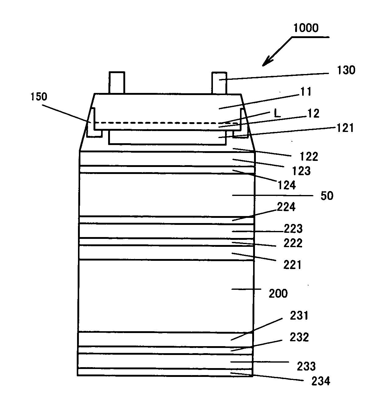
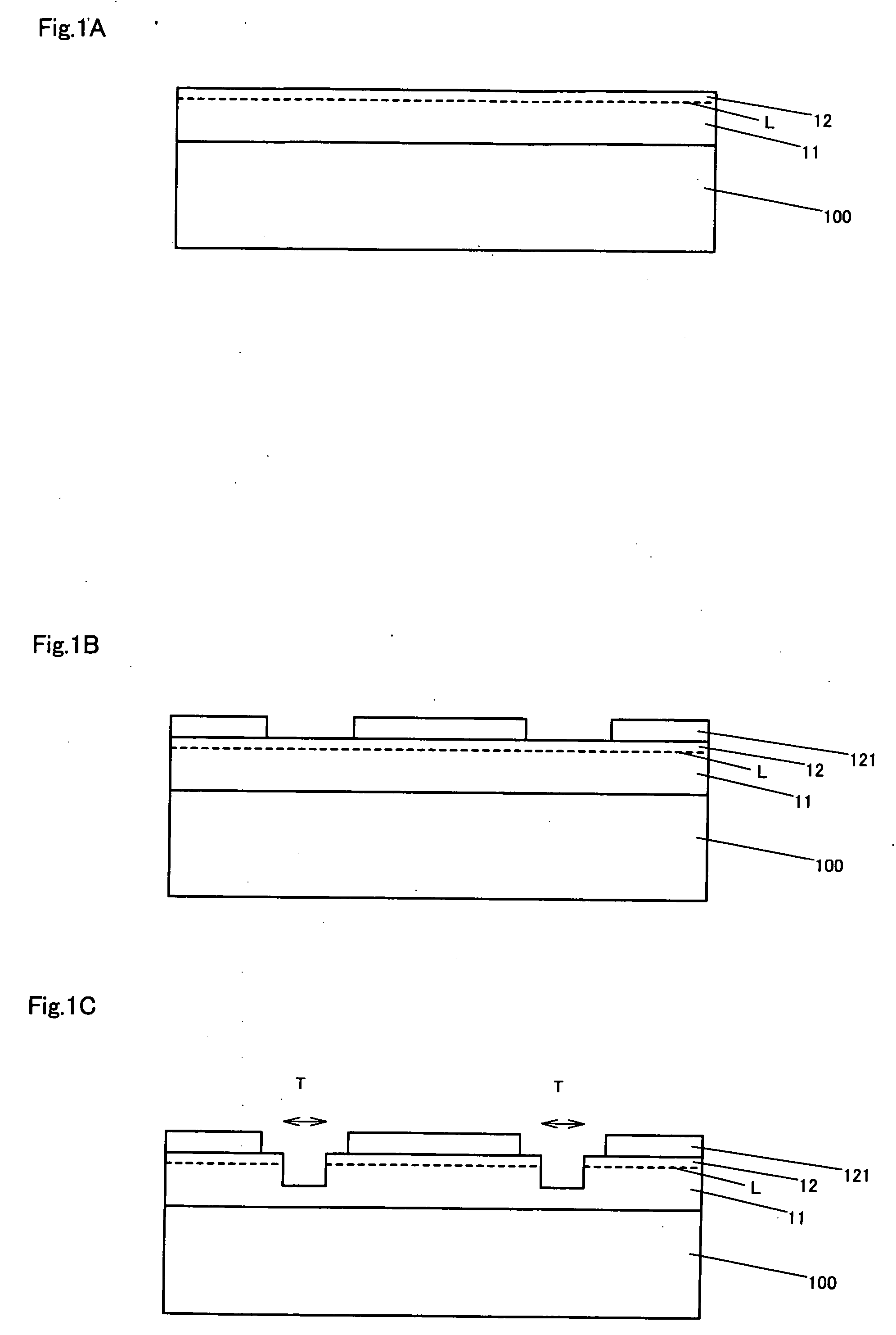
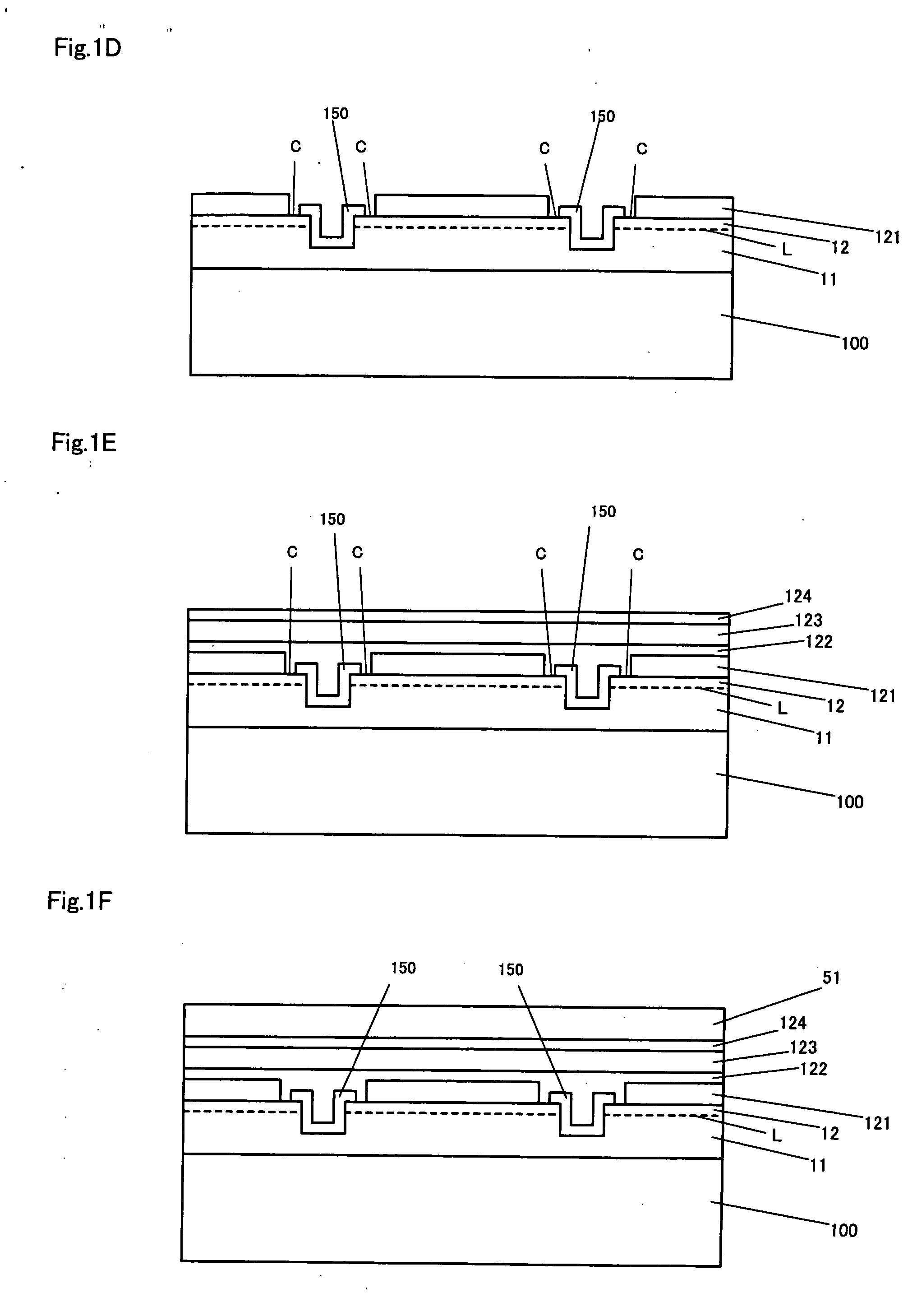
[0041]FIGS. 1A to 1J show cross-sections of a group III nitride based compound semiconductor light-emitting device 1000 in the production steps according to one embodiment of the present invention. FIG. 1J shows one chip of the group III nitride based compound semiconductor light-emitting device 1000. FIGS. 1A to 1I show cross-sections of about three chips of the device, and enlarged cross-sections of one single wafer.
[0042] Firstly, a sapphire substrate 100 is provided, and a group III nitride based compound semiconductor layer is formed on the substrate through routine epitaxial growth (FIG. 1A). FIG. 1A shows the group III nitride based compound semiconductor layer as a simplified stacked structure including an n-type layer 11 and a p-type layer 12 with a light-emitting region L. In FIGS. 1A to 1J, the n-type layer 11 and the p-type layer 12 are shown as two layers in contact with each other at the light-emitting region L represented by a broken line, and detailed stacked struct...
PUM
 Abstract
Description
Claims
Application Information