Semiconductor device

a technology of semiconductor devices and semiconductors, applied in semiconductor devices, semiconductor/solid-state device details, electrical apparatus, etc., can solve the problems of reducing radiation efficiency, warpage of resin packages during hardening, and the inability to reference 1 , to achieve the effect of reducing the warpage of resin packages

Active Publication Date: 2007-06-21
MITSUBISHI ELECTRIC CORP
View PDF12 Cites 38 Cited by
  • Summary
  • Abstract
  • Description
  • Claims
  • Application Information

AI Technical Summary

Benefits of technology

[0013]In the semiconductor device so structured, the warpage of the resi

Problems solved by technology

Unlike the case-type semiconductor device, the mold-type semiconductor device can eliminate manufacturing steps for securing the case on the insulating substrate and for filling in the case with gel resin, but it may have a problem that the resin package warps during hardening due to difference of linear thermal expansion coefficients between the resin package and various components such as the radiating plate and the semiconductor chip covered by the resin package.
This may cause breakdown of the insulating substrate covered by the resin package, or may define a gap between the warped radiating plate and the

Method used


Image

  • Semiconductor device
  • Semiconductor device
  • Semiconductor device

Examples


embodiment 1

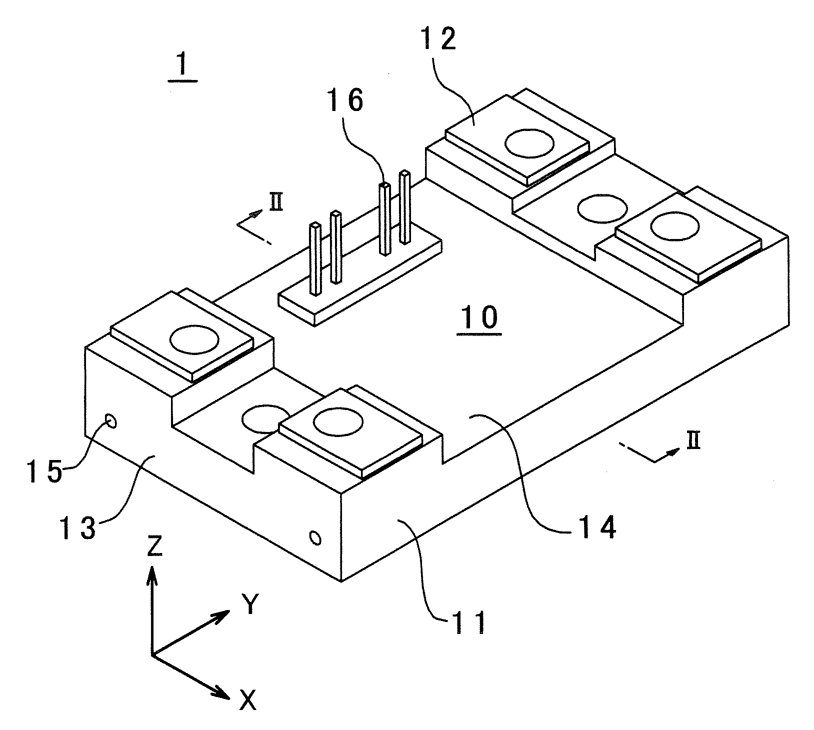
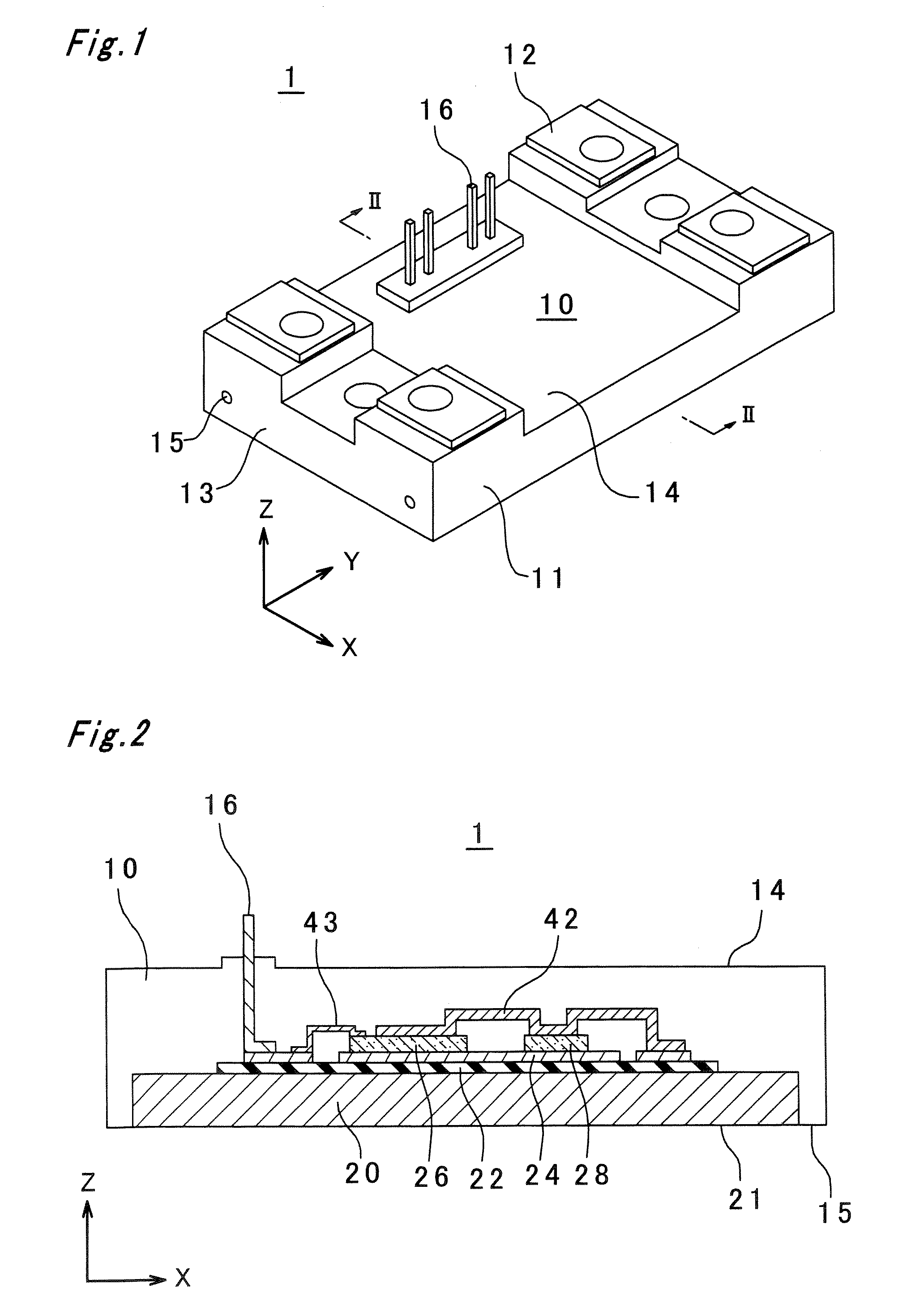
[0036]Referring to FIGS. 1-6, a mold-type semiconductor device according to the first embodiment of the present invention will be described herein. The semiconductor device 1 illustrated in FIG. 1 includes, in general, a resin package 10 formed by injection-molding with the thermoplastic resin, a plurality of main terminals 12 on the resin package 10, and a plurality of signal terminals 16 extending from the top surface 14 of the resin package 10. Although the resin package 10 of the present invention is preferably made of thermoplastic resin including, for example, polyphenylene sulfide (PPS) mixed with reinforcing material such as fiber glass, other thermoplastic resin can be used including polybutylene terephthalate (PBT) resin and liquid crystal polymer (LCP).

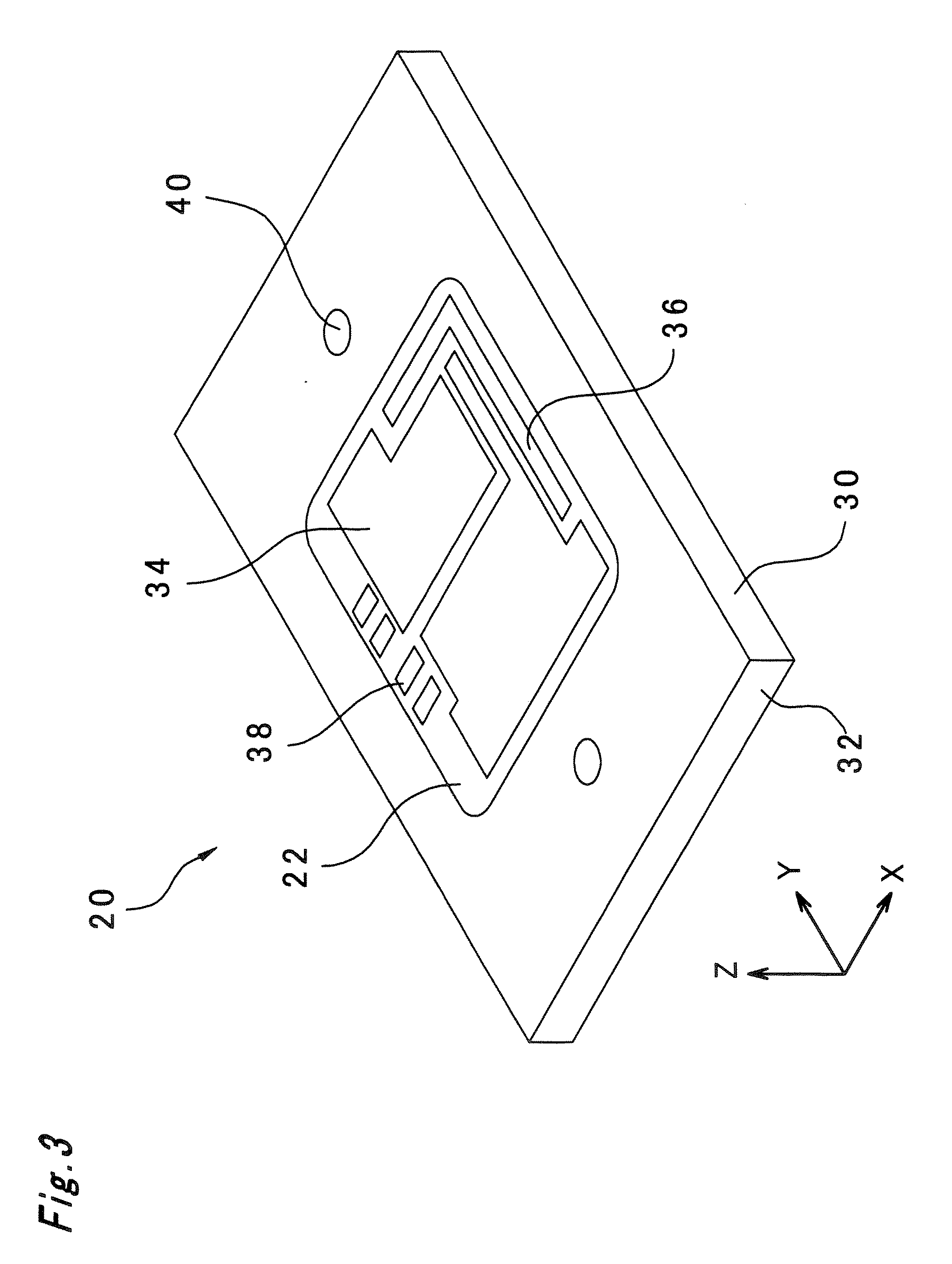
[0037]Also, the semiconductor device 1 of the present embodiment includes a radiating plate (base plate) 20, a wiring patterned layer 24 secured on the radiating plate via an insulating layer 22, and at least one semiconduc...

embodiment 2

[0062]Referring to FIG. 7, a semiconductor device according to the second embodiment of the present invention will be described herein. The semiconductor device 2 of the second embodiment has components similar to those of the first embodiment except that the resin package 10 has a transverse rib 46 provided on the top surface 14 thereof extending in parallel to the conductive lead plate 42. Therefore, no duplicate description will be made for the similar components of the second embodiment, which are denoted with similar reference numerals.

[0063]As above, according to the second embodiment, the semiconductor device 2 includes one or more transverse ribs 46 (three of ribs shown in FIG. 7) formed integrally with the top surface 14 of the resin package 10, which extend in parallel to the conductive lead plate 42 in the transverse direction (X-direction). Although the present invention is not limited by size of the transverse rib 46, for example, it may be sized with 2 mm (width) and 2...

embodiment 3

[0065]Referring to FIGS. 8-10, a semiconductor device according to the third embodiment of the present invention will be described herein. The semiconductor device 3 of the third embodiment has components similar to those of the first embodiment except that the radiating plate 20 includes a pair of longitudinal grooves 48 which are formed adjacent opposing ends 30 thereof extending in the longitudinal direction, and filled in with the resin package 10. Therefore, no duplicate description will be made for the similar components of the third embodiment, which are denoted with similar reference numerals.

[0066]In the semiconductor device 3 of FIGS. 8 and 9, since most of fiber glass in the resin package 10 is oriented along the longitudinal direction (Y-direction), the maximum anisotropy of the linear thermal expansion coefficient of the resin package 10 is realized in the transverse direction (X-direction), similar to the first embodiment. Also, the conductive lead plate 42 having the ...


PUM


Abstract

One of the aspects of the present invention is to provide a semiconductor device, which includes a radiating plate, a wiring patterned layer on the radiating plate via an insulating layer, at least one semiconductor chip mounted on the wiring patterned layer. The semiconductor chip has a surface electrode. The semiconductor device further includes a conductive lead plate electrically connected with the surface electrode of the semiconductor chip, and a resin package of thermoplastic resin having anisotropic linear expansion coefficient varying based upon directions. The resin package covers the wiring patterned layer, the semiconductor chip, the conductive lead plate, and at least a portion of the radiating plate. The conductive lead plate extends in a direction which provides the resin package with the maximum linear expansion coefficient. In the semiconductor device so structured, the warpage of the resin package is reduced both in longitudinal and transverse directions.

Description

BACKGROUND OF THE INVENTION[0001]1) Technical Field of the Invention[0002]The present invention relates to a semiconductor device, and in particular, relates to the semiconductor device having a resin package formed by molding with thermoplastic resin, which reduces warpage of the resin package.[0003]2) Description of Related Arts[0004]Conventional power semiconductor devices such as a power module are, in general, categorized into two types of semiconductor devices. That is, one is a case-type semiconductor device having a case which is filled up with gel resin after a semiconductor chip is mounted on an insulating substrate in the case, and another one is a mold-type semiconductor device having a resin package which is molded with resin covering the semiconductor chip mounted on the insulating substrate. Also, the mold-type semiconductor device is further grouped into two of sub-groups, i.e., one formed by transfer-molding with thermosetting resin and another made by injection-mol...

Claims


Application Information

Patent Timeline
IPC IPC(8): H01L23/34
CPCH01L23/3121H01L23/3735H01L2924/1305H01L2224/40137H01L2924/01028H01L2924/1815H01L2924/014H01L23/4334H01L24/36H01L24/40H01L24/45H01L24/84H01L25/072H01L25/18H01L2224/45124H01L2224/48091H01L2924/01002H01L2924/01013H01L2924/01014H01L2924/01029H01L2924/01033H01L2924/01047H01L2924/0105H01L2924/01074H01L2924/01079H01L2924/01082H01L2924/12044H01L2924/13055H01L2924/13091H01L2924/14H01L24/48H01L2924/01005H01L2924/01006H01L2924/01019H01L2924/01023H01L2924/00014H01L2924/00H01L2224/45015H01L2924/181H01L2224/40095H01L2224/40139H01L2224/40225H01L2224/4103H01L24/41H01L2224/0603H01L2224/371H01L2224/84801H01L2224/37147H01L24/37H01L2224/83801H01L2924/00012H01L2224/73221H01L23/28
Inventor SUDO, SHINGOOTA, TATSUOTANIGUCHI, NOBUTAKEYOSHIDA, HIROSHIKASHIMOTO, HIRONORI
Owner MITSUBISHI ELECTRIC CORP
Why Eureka
Try Eureka