Electronic carrier board and package structure thereof

a technology of electronic carrier board and package structure, which is applied in the direction of printed circuit aspects, sustainable manufacturing/processing, final product manufacturing, etc., can solve the problems of not being able to further reduce in size, occupying a significant amount of space, and not being able to use relatively large electronic components. , to achieve the effect of smooth flow through the groov

Inactive Publication Date: 2007-06-21
SILICONWARE PRECISION IND CO LTD
View PDF3 Cites 8 Cited by
  • Summary
  • Abstract
  • Description
  • Claims
  • Application Information

AI Technical Summary

Benefits of technology

[0015] In view of the above drawbacks of the prior art, a primary objective of the present invention is to provide an electronic carrier board and a package structure thereof, allowing a space between an electronic component and the electronic carrier board to be effectively filled with an epoxy molding compound (EMC), so as to avoid a void-induced popcorn effect and undesirable electrical bridging.
[0016] Another objective of the present invention is to provide an electronic carrier board and a package structure thereof, so as to prevent electrical short circuit between adjacent electronic components.
[0017] Still another objective of the present invention is to provide an electronic carrier board and a package structure thereof, allowing a conductive material, which connects an electronic component to the electronic carrier board, to be effectively encapsulated by an EMC, so as to prevent overflow and diffusion of the conductive material.
[0018] A further objective of the present invention is to provide an electronic carrier board and a package structure thereof, allowing an EMC encapsulating an electronic component on the electronic carrier board to flow through a groove under the electronic component without the occurrence of voids.
[0021] Therefore, in the electronic carrier board and the package structure thereof according to the present invention, a protective layer covering the electronic carrier board is formed with an opening corresponding to at least one pair of bond pads to expose at least three sides of each of the paired bond pads, and the protective layer includes at least one independent residual portion located in the opening and between the paired bond pads, wherein the independent residual portion is not in contact with the rest of the protective layer. Thus, when an electronic component is mounted on the independent residual portion and is electrically connected to the bond pads via a conductive material as well as is encapsulated by an EMC, the EMC may smoothly flow through the opening under the electronic component to thereby effectively fill the opening and a clearance between the electronic component and the electronic carrier board, such that a void-induced popcorn effect and undesirable electrical bridging are prevented.
[0023] Further in the present invention, since the protective layer has at least one independent residual portion located in the opening and between the paired bond pads and being not in contact with the rest of the protective layer, when the electronic component is mounted on the independent residual portion and is electrically connected to the bond pads via the conductive material as well as is encapsulated by the EMC, a groove without any dead space is provided between the electronic component and the electronic carrier board to allow the EMC to smoothly flow through the groove and fill the clearance between the electronic component and the electronic carrier board. This arrangement prevents the occurrence of turbulence of the EMC and thus solves the problem of voids and a popcorn effect caused by turbulence of the EMC occurring at corners of a small groove under an electronic component.

Problems solved by technology

The electronic components used in the THT, as not able to be further reduced in size, are considered occupying a significant amount of space on the electronic carrier board.
As it becomes necessary to mount passive components (such as capacitors, resistors or inductors) on an electronic carrier board to maintain stable electrical quality of an electronic product, and the electronic product is being made compact in size and with low consumption of power, the THT using relatively large electronic components is not considered suitable and is gradually replaced by the SMT.
This is because in the THT, through holes need to be formed in a circuit board to accommodate the pins of the electronic components and are spaced apart from each other by a distance corresponding to a pitch between the pins, and the electronic components with the pins coupled to the through holes occupy both sides of the circuit board, thereby leading to unsatisfactory space utilization of the circuit board.
However, it is found difficult to accurately control the height of the passive component 14 bonded to the solder paste 15 due to the amount of the solder paste 15 being used and melting of the solder paste 15 in the reflow soldering process.
The voids result in a popcorn effect in a subsequent high-temperature operating environment, which undesirably damages the whole package structure.
Furthermore, the melting solder paste 15 may flow into the clearance 17 (by a capillary action) and lead to undesirable electrical bridging and short circuit of the passive component 14 (as shown in FIG. 1B), thereby adversely affecting the yield of the fabricated package structure.
By such arrangement, it is even more difficult to fill the clearance between the passive component and the substrate with the EMC but easier for the occurrence of the solder extrusion.
Therefore, the problem to be solved here is to provide an electronic carrier board and a package structure thereof, which can avoid formation of voids, electrical bridging and solder extrusion in the presence of a clearance formed between the electronic carrier board and an electronic component mounted thereon.

Method used


Image

  • Electronic carrier board and package structure thereof
  • Electronic carrier board and package structure thereof
  • Electronic carrier board and package structure thereof

Examples


first preferred embodiment

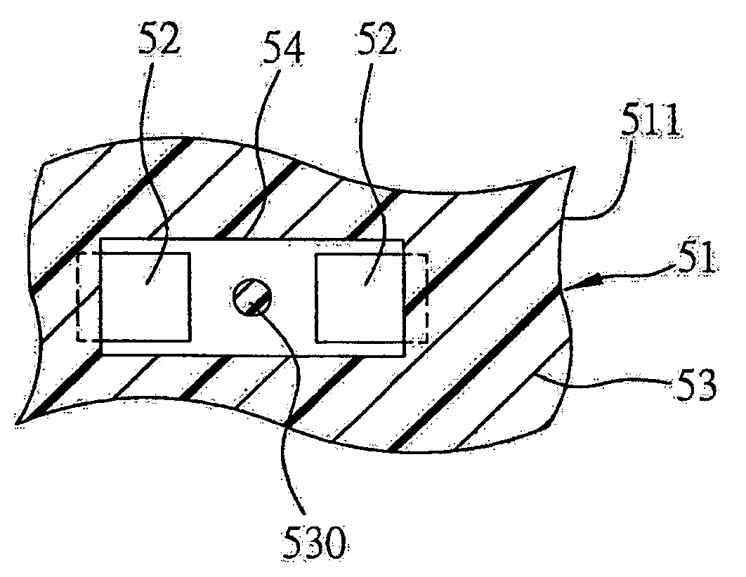
[0037]FIGS. 5A and 5B are top views of an electronic carrier board and an electronic component mounted thereon according to a first preferred embodiment of the present invention.

[0038] Referring to FIGS. 5A and 5B, the electronic carrier board 51 of the present invention comprises: a carrier 511; a plurality of bond pads, including at least one pair of bond pads 52, formed on a surface of the carrier 511; and a protective layer 53 covering the surface of the carrier 511. The protective layer 53 is formed with an opening 54 corresponding to the at least one pair of bond pads 52 to expose at least three sides of each of the paired bond pads 52. And the protective layer 53 includes at least one independent residual portion 530 located in the opening 54 and between the paired bond pads 52.

[0039] The electronic carrier board 51 can be a package substrate used for chip packaging, a circuit board, or a printed circuit board, etc. In this embodiment, the package substrate is described. Th...

second preferred embodiment

[0045]FIG. 7 is a top view of an electronic carrier board according to a second preferred embodiment of the present invention.

[0046] The electronic carrier board and a package structure thereof of this second embodiment are similar to those of the first preferred embodiment, with a primary difference in that, in the second embodiment, the protective layer 53 includes a plurality of independent residual portions 530 located in the opening 54 and between the at least one pair of bond pads 52. Two independent residual portions are shown in FIG. 7 but do not set a limitation for the present invention. These independent residual portions 530 are not in contact with the rest of the protective layer 53. By such arrangement, the electronic component can be well supported by the independent residual portions 530 and the EMC 57 can smoothly flow through the groove without the dead space under the electronic component and fill the space under the electronic component.

third preferred embodiment

[0047]FIG. 8 is a top view of an electronic carrier board according to a third preferred embodiment of the present invention.

[0048] The electronic carrier board and a package structure thereof of this third embodiment are similar to those of the first preferred embodiment, with a primary difference in that, in the third embodiment, the protective layer 53 includes a plurality of independent residual portions 530 located in the opening 54 and between the at least one pair of bond pads 52. Two independent residual portions are shown in FIG. 7 but do not set a limitation for the present invention. These independent residual portions 530 come into contact with the bond pads 52 but are not in contact with the rest of the protective layer 53. By such arrangement, the electronic component can be well supported by the independent residual portions 530 and the EMC 57 can smoothly flow through the groove without the dead space under the electronic component and fill the space under the elect...


PUM


Abstract

An electronic carrier board and a package structure thereof are provided. The electronic carrier board includes a carrier, at least one pair of bond pads formed on the carrier, and a protective layer covering the carrier. An opening is formed in the protective layer to expose at least three sides of each of the paired bond pads. The protective layer includes at least one independent residual portion located in the opening and between the paired bond pads, such that an electronic component is mounted on the independent residual portion and electrically connected to the bond pads. A groove without a dead space is formed between the electronic component and the carrier, such that a molding compound for encapsulating the electronic component can flow through the groove to fill the opening and a space under the electronic component and encapsulate the at least three sides of each of the bond pads.

Description

FIELD OF THE INVENTION [0001] The present invention relates to electronic carrier boards and package structures thereof, and more particularly, to an electronic carrier board applicable to surface mounted technology (SMT) and a package structure having the electronic carrier board. BACKGROUND OF THE INVENTION [0002] Electronic components have been continuously designed and fabricated to have a miniaturized profile in response to the progress of integrated circuit (IC) manufacturing technology, and with provision of large-scale and highly integrated electronic circuits, IC-based products have relatively complete functionality. [0003] Conventionally, electronic components are mounted on an electronic carrier board (such as a printed circuit board (PCB), a circuit board, or a substrate) by through hole technology (THT). The electronic components used in the THT, as not able to be further reduced in size, are considered occupying a significant amount of space on the electronic carrier b...

Claims


Application Information

Patent Timeline
Patent Type & Authority Applications(United States)
IPC IPC(8): H01L23/34
CPCH05K3/284H05K3/303H05K3/3452H05K2201/0989H05K2201/10636H05K2201/10727H05K2201/2036Y02P70/50
Inventor TSAI, FANG-LINTSAI, HO-YIHUANG, CHIH-MINGHUANG, CHIEN-PINGHSIAO, CHENG-HSU
Owner SILICONWARE PRECISION IND CO LTD
Why Eureka
Try Eureka