Low temperature doped silicon layer formation

a technology of silicon layer and low temperature, applied in the field of forming doped silicon layers, can solve the problems of reducing the film deposition rate, falling to unacceptably low levels, and the rate of falling so low

Active Publication Date: 2007-06-21
ASM INTERNATIONAL
View PDF99 Cites 27 Cited by
  • Summary
  • Abstract
  • Description
  • Claims
  • Application Information

AI Technical Summary

Problems solved by technology

However, the deposition rate of the film strongly decreases with temperature and can fall to unacceptably low levels.
In particular, the deposition rate can fall so low that the processing becomes uneconomical.
Moreover, there exist limits to the extent that smoothness can be increased by lowering the deposition temperature.
This problem is particularly acute in the case of n-type doped films such as phosphorus doped films.
However, n-type dopants are known...

Method used


Image

  • Low temperature doped silicon layer formation
  • Low temperature doped silicon layer formation
  • Low temperature doped silicon layer formation

Examples


example 2

[0076] A doped silicon layer was deposited on a batch of substrates in a batch reactor. The reactor was an A412™ from ASM International N.V. of Bilthoven, The Netherlands. The process chamber pressure was 200 mTorr and the deposition temperature 450° C. A 60 sccm trisilane flow was mixed with a 1 slm N2 carrier gas flow before introduction into the process chamber and a 60 sccm N2 flow comprising 1% phosphine was used to provide the dopant precursor. The deposition rate was 2.4 Å / min and the phosphorus incorporation 2.1×10²⁰ atoms / cm3. The deposition formed doped silicon films having a thickness of about 150 Å or less and, more preferably, about 100 Å or less.

Example 3

[0077] A doped silicon layer was deposited on a batch of wafers in a batch reactor. Seventy-five product wafers having a diameter of 300 mm were held on holder rings in a wafer boat in the process chamber of an A412™ reactor. The trisilane was flowed at 400 sccm, PH3 (1% in N2) was flowed at 400 sccm, N2 was flowed a...

example 3

[0078] A doped silicon layer was deposited on a batch of wafers in a batch reactor. Seventy-five product wafers having a diameter of 300 mm were held on holder rings in a wafer boat in the process chamber of an A412™ reactor. The trisilane was flowed at 400 sccm, PH3 (1% in N2) was flowed at 400 sccm, N2 was flowed at 200 sccm into the process chamber. The process chamber pressure was 200 mTorr and the temperature was 500° C. A deposition rate of 45 Å / min was achieved and the resulting film had a RMS roughness of 3.25 nm.

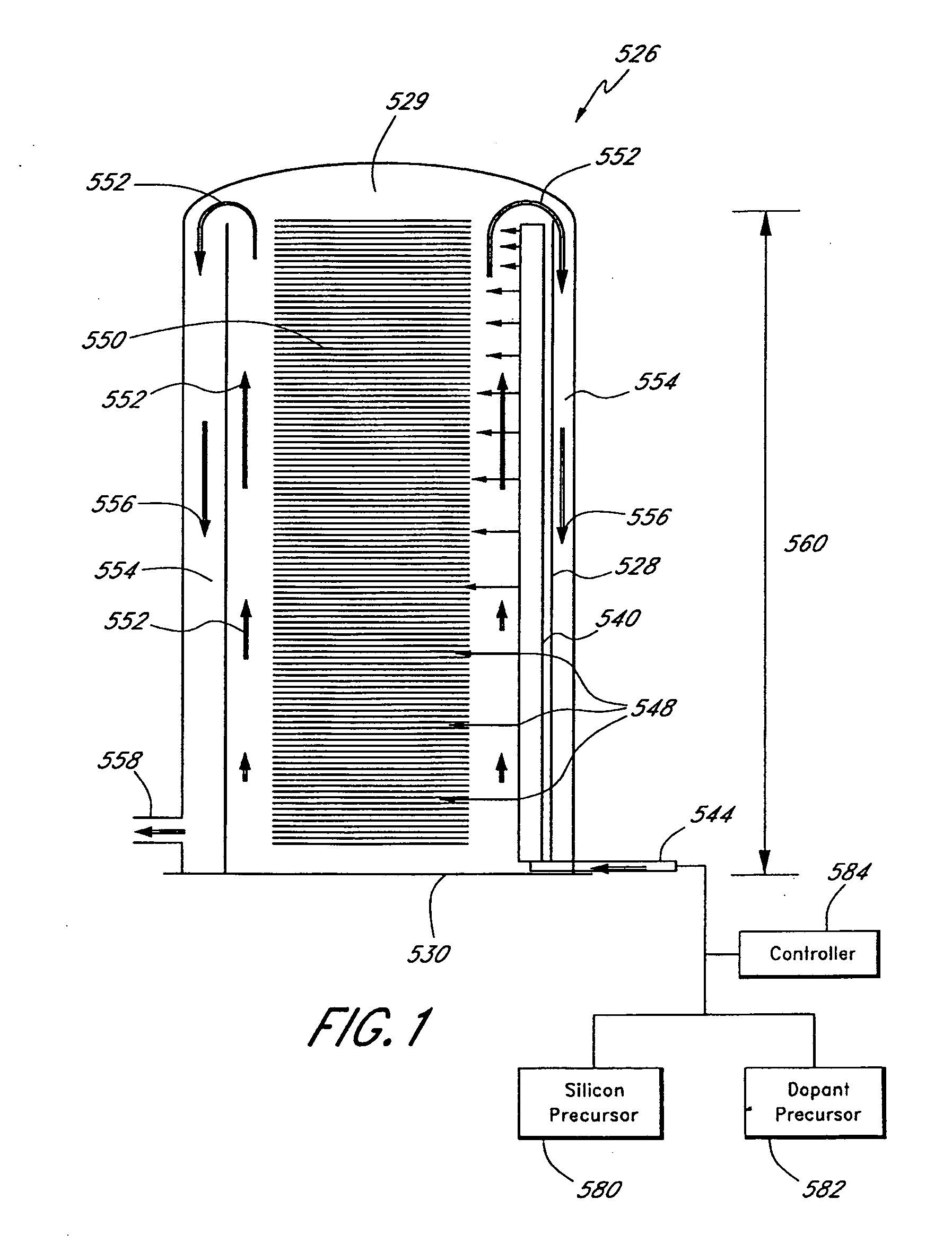
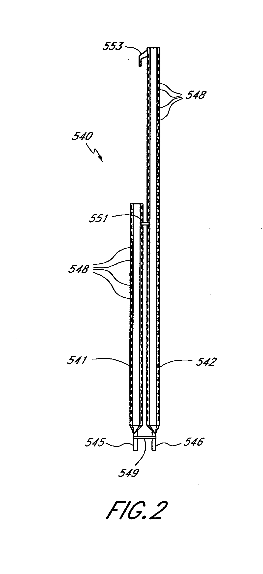
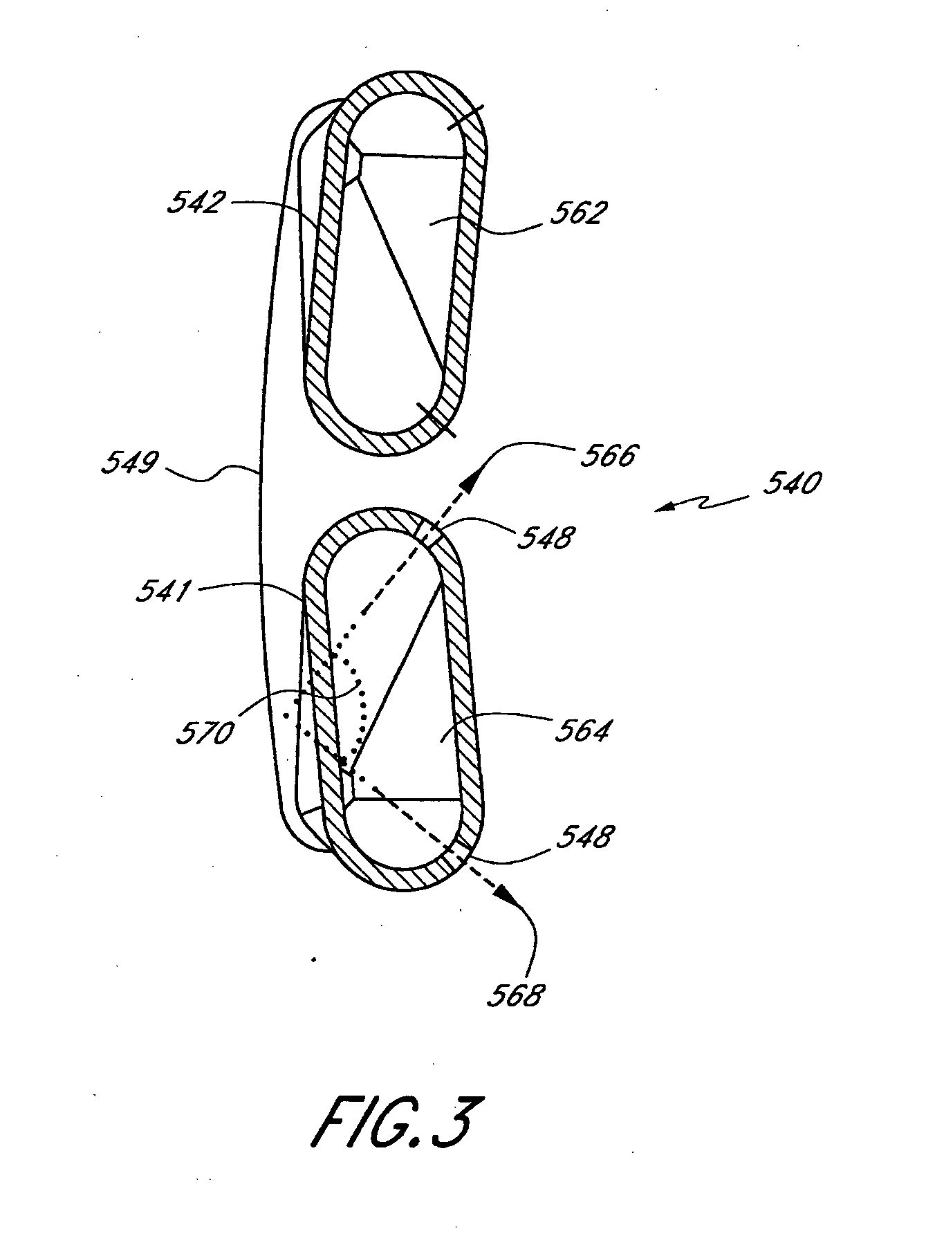
[0079] It will be appreciated that, while described with reference to various illustrated embodiments for ease for description, changes to the illustrated embodiments are possible. For example, the depositions can be performed in a reactor without a liner. In some arrangements, in such a reactor, process gases can be flowed into the reactor chamber at one vertical end and exhausted from the reactor at the opposite vertical end. In other arrangements, process gases ...


PUM

PropertyMeasurementUnit
Temperatureaaaaaaaaaa

Abstract

A doped silicon layer is formed in a batch process chamber at low temperatures. The silicon precursor for the silicon layer formation is a polysilane, such as trisilane, and the dopant precursor is an n-type dopant, such as phosphine. The silicon precursor can be flowed into the process chamber with the flow of the dopant precursor or separately from the flow of the dopant precursor. Surprisingly, deposition rate is independent of dopant precursor flow, while dopant incorporation linearly increases with the dopant precursor flow.

Description

PRIORITY CLAIM [0001] This application claims the priority benefit under 35 U.S.C. §119(e) of provisional Application No. 60 / 750,928, filed Dec. 16, 2005, entitled Low Temperature Doped Silicon Layer Formation. CROSS-REFERENCE TO RELATED APPLICATIONS [0002] In addition, this application is related to: U.S. patent application Ser. No. 11 / 213,449, filed Aug. 25, 2005 (Attorney Docket No. ASMINT.068AUS); U.S. patent application Ser. No. 10 / 623,482, filed Jul. 18, 2003 (Attorney Docket No. ASMEX.376A); U.S. Pat. No. 6,962,859, issued Nov. 8, 2005 (Attorney Docket No. ASMEX.333A); U.S. Pat. No. 6,821,825, issued Nov. 23, 2004 (Attorney Docket No. ASMEX.291A); and U.S. patent application Ser. No. 11 / 370,228, filed Mar. 6, 2006 (Attorney Docket No. ASMINT.081AUS), the disclosure of each of which is hereby incorporated by reference in its entirety.FIELD OF THE INVENTION [0003] This invention relates generally to semiconductor processing and, more particularly, to methods for forming doped s...

Claims


Application Information

Patent Timeline
IPC IPC(8): H01L21/20
CPCC23C16/24C23C16/45523C23C16/45578C30B25/02C30B29/06H01L21/02532H01L21/02576H01L21/0262
Inventor ZAGWIJN, PETER MARCOOSTERLAKEN, THEODORUS GERARDUS MARIAVAN AERDE, STEVEN R.A.FISCHER, PAMELA RENE
Owner ASM INTERNATIONAL
Why Eureka
Try Eureka