Microelectronic assemblies having very fine pitch stacking

a microelectronic and assembly technology, applied in the direction of semiconductor devices, semiconductor/solid-state device details, electrical apparatus, etc., can solve the problems of imposing stress on assemblies including packages, terminals moving relative to the contact, and imposing stress on solders, etc., to achieve the effect of facilitating testing

Active Publication Date: 2007-06-28
TESSERA INC
View PDF95 Cites 46 Cited by
  • Summary
  • Abstract
  • Description
  • Claims
  • Application Information

AI Technical Summary

Benefits of technology

[0038] Assemblies in accordance with certain preferred embodiments of the present invention facilitate testing of microelectronic elements and packages having non-planar contacts and interfaces, and avoids the need for specialized, expensive test equipment. In preferred ...

Problems solved by technology

Assemblies including packages can suffer from stresses imposed by differential thermal expansion and contraction of the device and the substrate.
Where the terminals of the package are fixed relative to the chip or other device, such as by using solder, these effects tend to cause the terminals to move relative to the contact pads on the circuit board.
This can impose stresses in the solder that connects the terminals to the contact pads on the circuit board.
Testing of packaged devices poses another formidable problem.
However, it is difficult to make connections by pressing the package against a simple test fixture such as an ordinary circuit board having planar contact pads.
For example, in a BGA package, differences in the diameter of the solder balls attached to the terminals, and non-planarity of the chip carrier, may cause some of the solder balls to lie at different heights.
However, such features add to the cost of the test fixture and, in some cases, introduce some unreliability into...

Method used


Image

  • Microelectronic assemblies having very fine pitch stacking
  • Microelectronic assemblies having very fine pitch stacking
  • Microelectronic assemblies having very fine pitch stacking

Examples


Embodiment Construction

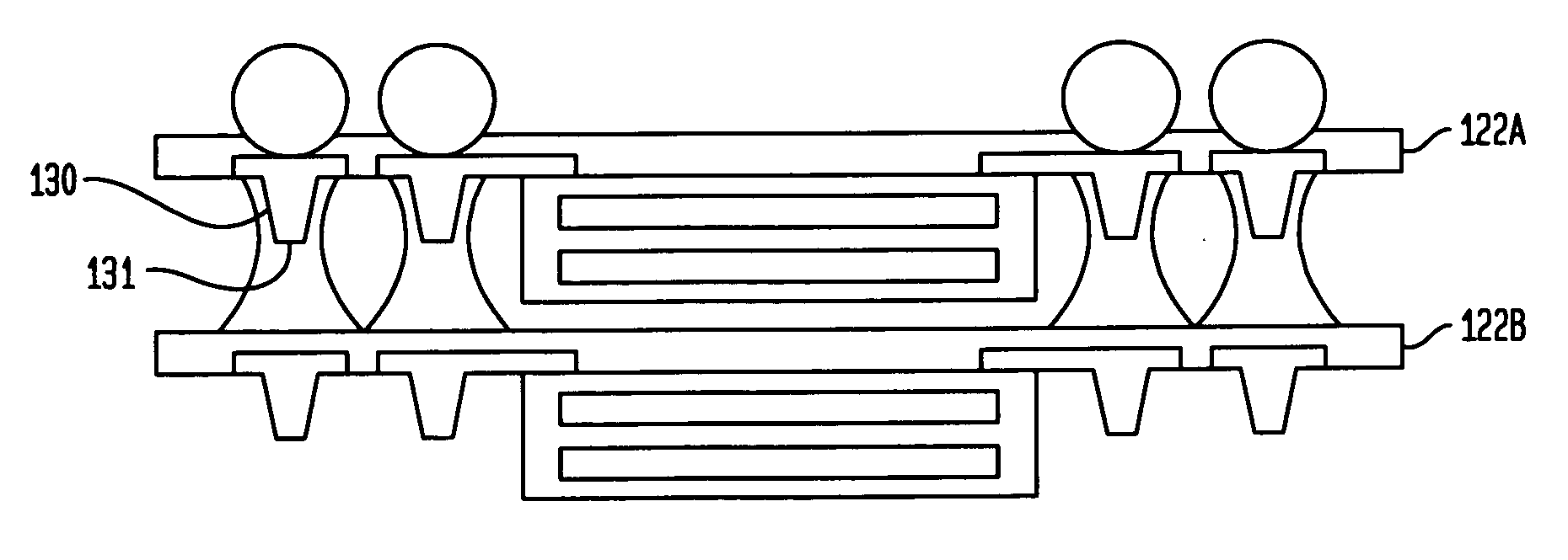
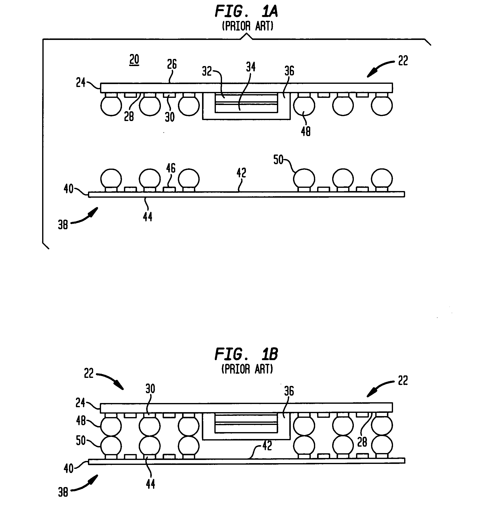
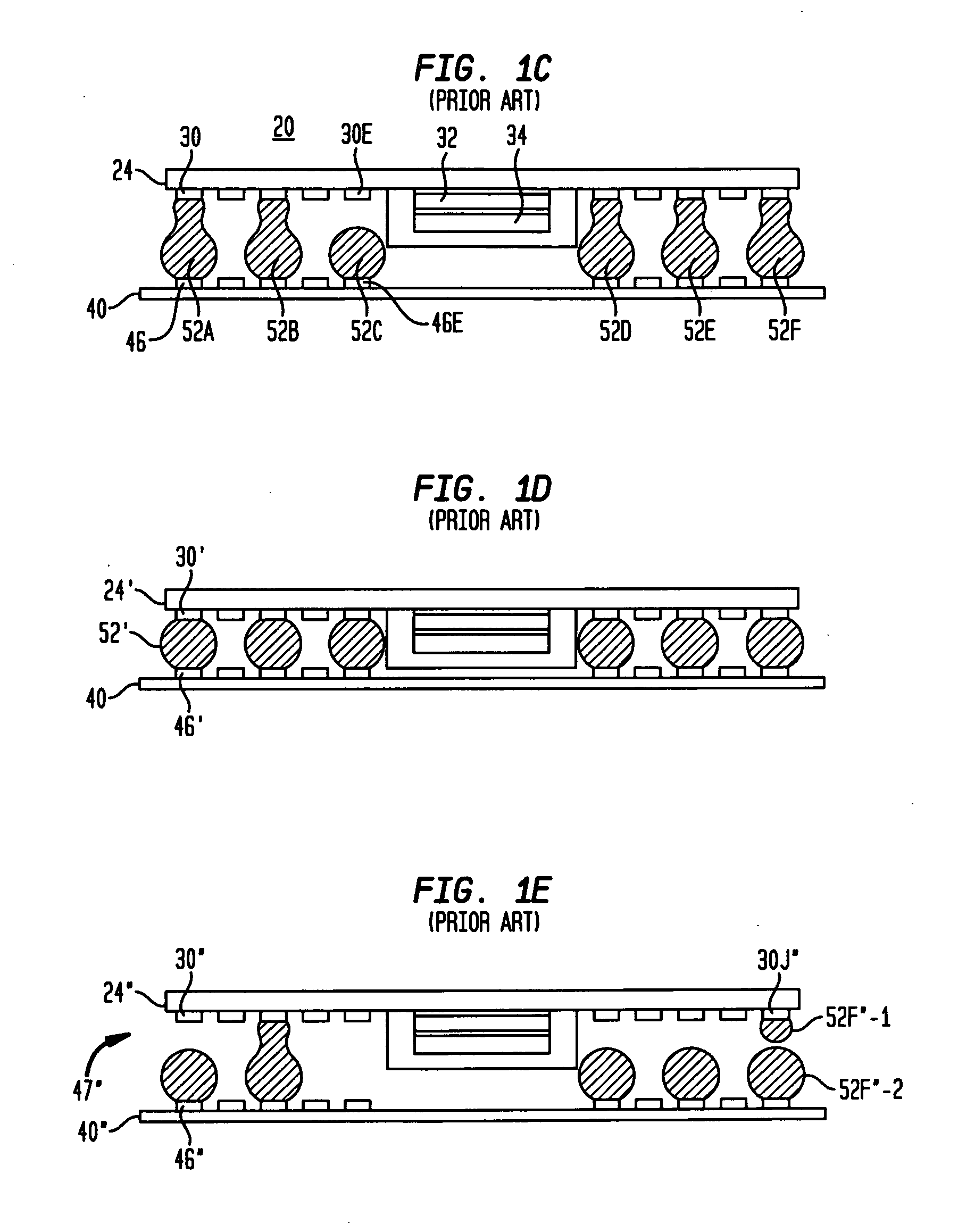
[0049]FIGS. 1A-1C show a conventional method of making a stackable assembly including a first microelectronic package 22 having a dielectric substrate 24 with a first surface 26 and a second surface 28. The first microelectronic package 22 includes conductive pads 30 accessible at the second surface 28 of the substrate 24. The first microelectronic package 22 also includes a first microelectronic element 32, such as a semiconductor chip, attached to the second surface 28 of the substrate 24. The microelectronic package 22 also includes a second microelectronic element 34 overlying the first microelectronic element 32. An encapsulating material 36 covers the first and second microelectronic elements 32, 34.

[0050] Referring to FIG. 1A, the microelectronic assembly also includes a second microelectronic element 38 including a substrate 40 having a first surface 42 and a second surface 44. The first surface 42 of the substrate 40 includes contacts 46 accessible at the first surface. Du...


PUM


Abstract

A microelectronic assembly includes two or more microelectronic packages stacked at a fine pitch, which is finer than the pitch that is possible when using solder balls for making the joint. Each stackable package desirably includes a substrate having pins projecting from one surface of the substrate and solder balls projecting from the other surface of the substrate. Each stackable package may have one or more die attached to one or more of the surfaces of the substrate. In certain embodiments, die may be attached to both surfaces of the substrate. The dies may be electrically interconnected with the substrate using wire bonds, flip chip bonding, leads and/or stud bumping. The die may be encapsulated in an encapsulated material, under-filled or glob topped. In certain preferred embodiments, the combination of the conductive post height and ball height is equal to or greater than the height of the encapsulated or molded chip structure. The combination of the conductive post height and the ball height must be at least equal to the height of the encapsulated chip structure so that the conductive elements are able to span the gap between layers of the assembly. After the tips of the conductive pads are in contact with the solder masses, the solder masses are reflowed to form a permanent electrical interconnection between the stacked microelectronic packages. During reflow, the reflowed solder will wick up around the conductive posts to form elongated solder columns. In addition, when the solder is reflowed, surface tension pulls the opposing layers of the assembly toward one another and provides a self-centering action for the conductive posts.

Description

[0001] The present invention relates to microelectronic assemblies and to methods of making and testing stackable microelectronic assemblies. BACKGROUND OF THE INVENTION [0002] Microelectronic devices such as semiconductor chips typically require many input and output connections to other electronic components. The input and output contacts of a semiconductor chip or other comparable device are generally disposed in grid-like patterns that substantially cover a surface of the device (commonly referred to as an “area array”) or in elongated rows which may extend parallel to and adjacent each edge of the device's front surface, or in the center of the front surface. Typically, devices such as chips must be physically mounted on a substrate such as a printed circuit board, and the contacts of the device must be electrically connected to electrically conductive features of the circuit board. [0003] Semiconductor chips are commonly provided in packages that facilitate handling of the chi...

Claims


Application Information

Patent Timeline
IPC IPC(8): H01L21/00H01L21/44
CPCH01L25/105H01L25/50H01L2924/15311H01L2924/1532H01L2924/15331H01L2924/3011H01L2924/3511H01L25/0657H01L2225/1023H01L2225/1058H01L2224/16H01L23/12
Inventor HABA, BELGACEMMITCHELL, CRAIG S.
Owner TESSERA INC
Why Eureka
Try Eureka