Method of forming fin transistor

a technology of fin transistor and field oxide layer, which is applied in the direction of semiconductor devices, basic electric elements, electrical appliances, etc., can solve the problems of difficult to form field oxide layer for isolating active regions from one another, difficult to obtain the required threshold voltage, and difficulty in obtaining the required threshold voltage. to achieve the effect of preventing undesired etching of sog layer

Inactive Publication Date: 2007-06-28
SK HYNIX INC
View PDF8 Cites 12 Cited by
  • Summary
  • Abstract
  • Description
  • Claims
  • Application Information

AI Technical Summary

Benefits of technology

[0009]Accordingly, the present invention has been made in an effort to solve the problems occurring in the related art, and an o...

Problems solved by technology

This causes difficulty in obtaining a required threshold voltage when a conventional transistor, which has a two-dimensional planar channel structure, is used in a highly integrated semiconductor device.
This also causes limitations in improving the refresh characteristics.
Meanwhile, as the degree of integration of a device increases, it has been difficult to form a field oxide layer for isolating active regions from one another.
Specifically, as the gap between field regions is narrowed, ...

Method used


Image

  • Method of forming fin transistor
  • Method of forming fin transistor
  • Method of forming fin transistor

Examples


Embodiment Construction

[0028]Reference will now be made in greater detail to a preferred embodiment of the invention, an example of which is illustrated in the accompanying drawings. Wherever possible, the same reference numerals will be used throughout the drawings and the description to refer to the same or like parts.

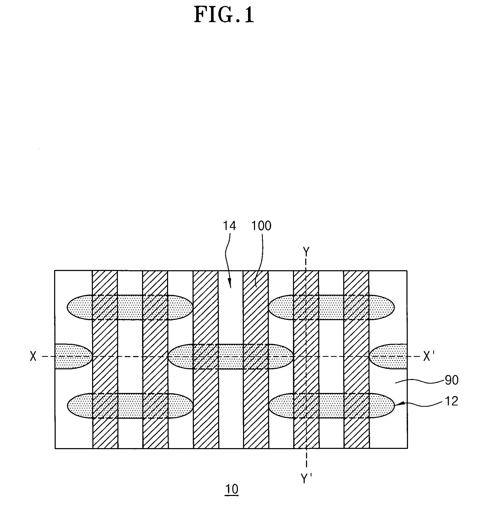
[0029]FIG. 1 is a plan view for explaining a method of forming a fin transistor in accordance with an embodiment of the present invention.

[0030]As illustrated in FIG. 1, a silicon substrate 10 has a plurality of active regions 12 and a field region 14 defining the active regions 12. A field oxide layer 90 is formed in the field region 14. The gate 100 is formed to dispose on the active region 12 and the field oxide layer 90.

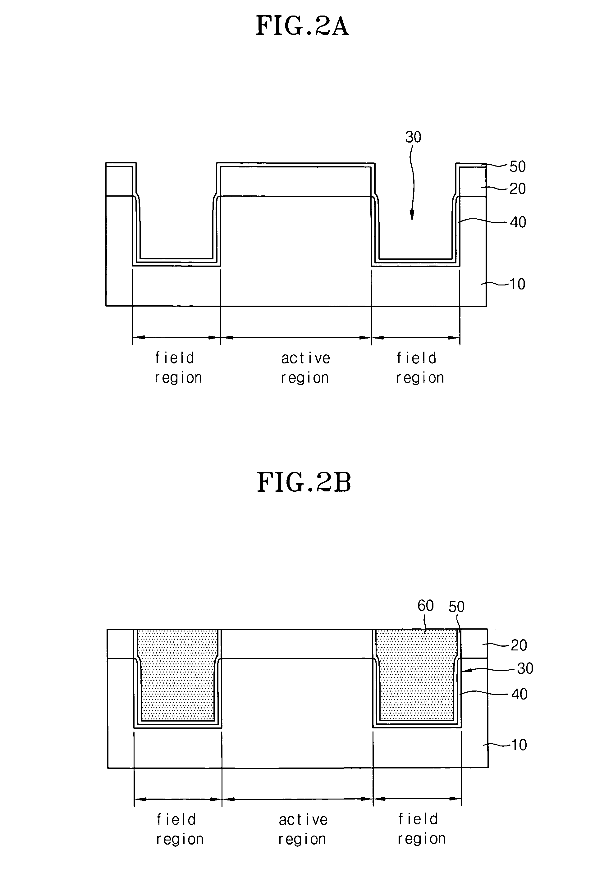
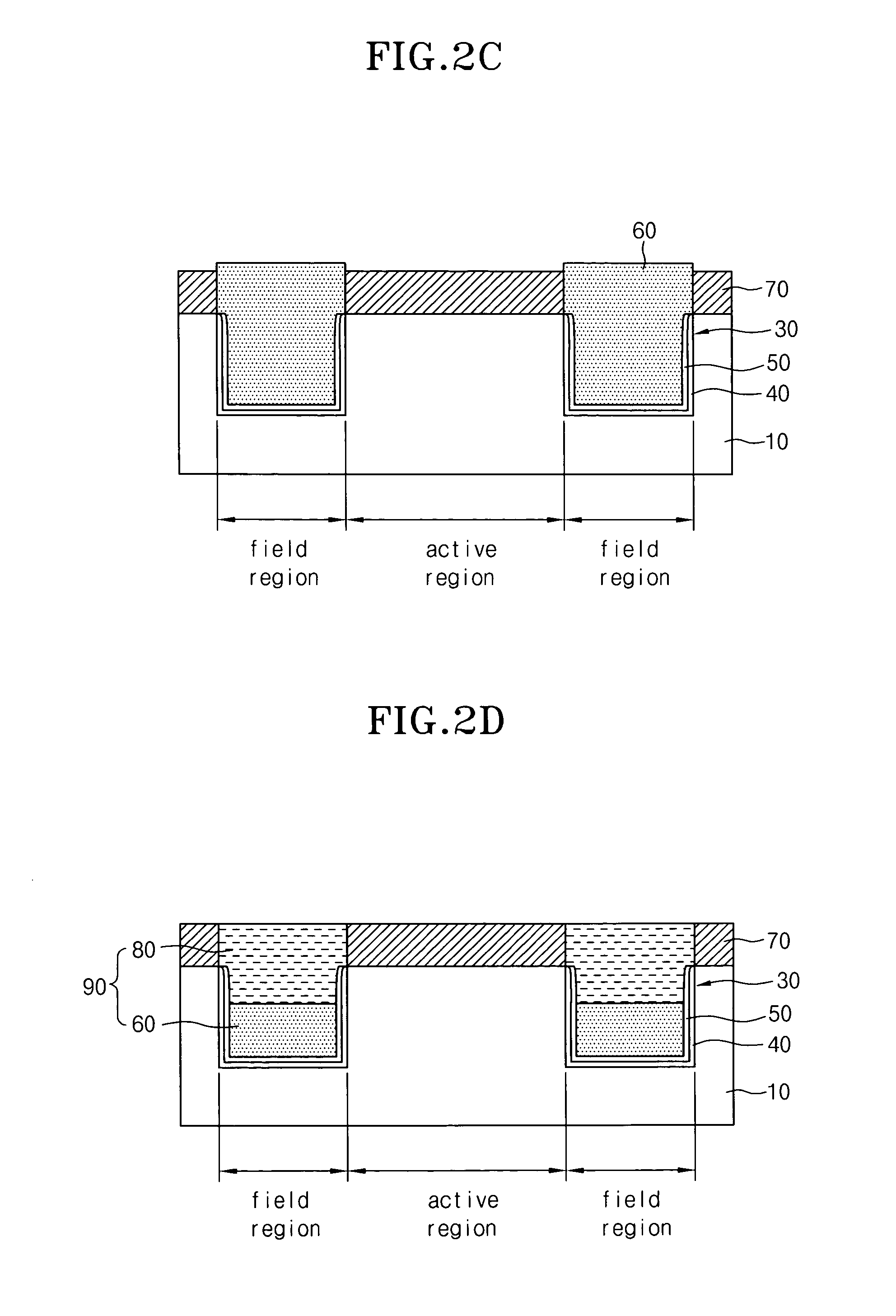
[0031]FIGS. 2A-2F are cross-sectional views taken along the lines X-X′ in FIG. 1 to show each cross-sectional view corresponding to one or more selected process steps. Similarly, FIGS. 3A-3F are cross-sectional views taken along the line Y-Y′ in FIG. 1 to show each cros...


PUM


Abstract

A fin transistor is formed by forming a hard mask layer on a substrate having an active region and a field region. The hard mask layer is etched to expose the field region. A trench is formed by etching the exposed field region. The trench is filled with an SOG layer. The hard mask layer is removed to expose the active region. An epi-silicon layer is formed on the exposed active region. The SOG layer is then partially etched from the upper end of the trench, thus filling a lower portion of the trench. A HDP oxide layer is deposited on the etched SOG layer filling the trench, thereby forming a field oxide layer composed of the SOG layer and the HDP oxide. The HDP oxide layer in the field oxide layer is etched to expose both side surfaces of the epi-silicon layer. A gate is then formed on the epi-silicon layer of which both side surfaces are exposed and the field oxide layer.

Description

BACKGROUND OF THE INVENTION[0001]1. Field of the Invention[0002]The present invention relates to a method of manufacturing a semiconductor device, and more particularly to a method of forming a fin transistor, which is constructed to improve performance and yield in a semiconductor device.[0003]2. Description of the Related Art[0004]The design rule calling for increasingly shrinking semiconductor memory device in terms of size means that the channel length and the channel width of a transistor formed therein must decrease while both the doping concentration of the junction regions and the junction leakage current increase due to formation of high electric field. This causes difficulty in obtaining a required threshold voltage when a conventional transistor, which has a two-dimensional planar channel structure, is used in a highly integrated semiconductor device. This also causes limitations in improving the refresh characteristics.[0005]In response to these problems, some known rese...

Claims


Application Information

Patent Timeline
IPC IPC(8): H01L21/8234
CPCH01L21/823437H01L29/66795H01L29/7851H01L21/18
Inventor SHEEN, DONG SUNSONG, SEOK PYOAHN, SANG TAESOHN, HYUN CHUL
Owner SK HYNIX INC
Why Eureka
Try Eureka