Multi-path accessible semiconductor memory device

a memory device and multi-path technology, applied in the field of semiconductor memory devices, can solve the problems of increased size complexity, increased cost in configuring memories, and difficulty in obtaining satisfactory data transmission speeds

Inactive Publication Date: 2007-06-28
SAMSUNG ELECTRONICS CO LTD
View PDF10 Cites 15 Cited by
  • Summary
  • Abstract
  • Description
  • Claims
  • Application Information

AI Technical Summary

Benefits of technology

[0017]A semiconductor memory device includes ports, data line pairs, where each port associated with one of the data line pairs, sets of address lines, where each port associated with one of the sets of address lines, a shared memory region of a memory cell array, where the shared memory region accessible through the ports, an access controller coupled to the ports and configured to generate an access selection signal in response to a plurality of control signals received through the ports, and an access router coupled to the shared memory region, the data line pairs, and the sets of address lines, the access router configured to selectively couple one of the sets of address lines and one of the data line pairs to the shared memory region in response to the access selection signal.
[0018]Another embodiment includes a method of operating a semiconductor memory device including receiving a plurality of addresses through a plurality of ports, each address associated with an access through an associated port, generating an access selection signal in response to a plurality of control signals received through the ports, selecting an address from among the addresses for access to a shared memory region in response to the access selection signal, forming a data input / output path between a port associated with the selected address and the shared memory region in response to the access selection signal, and accessing data in the shared memory region through the data input / output path.

Problems solved by technology

Thus, it is difficult to obtain a satisfactory data transmission speed and size complexity is increased.
Furthermore, there is an increased cost in configuring memories.

Method used


Image

  • Multi-path accessible semiconductor memory device
  • Multi-path accessible semiconductor memory device
  • Multi-path accessible semiconductor memory device

Examples


Embodiment Construction

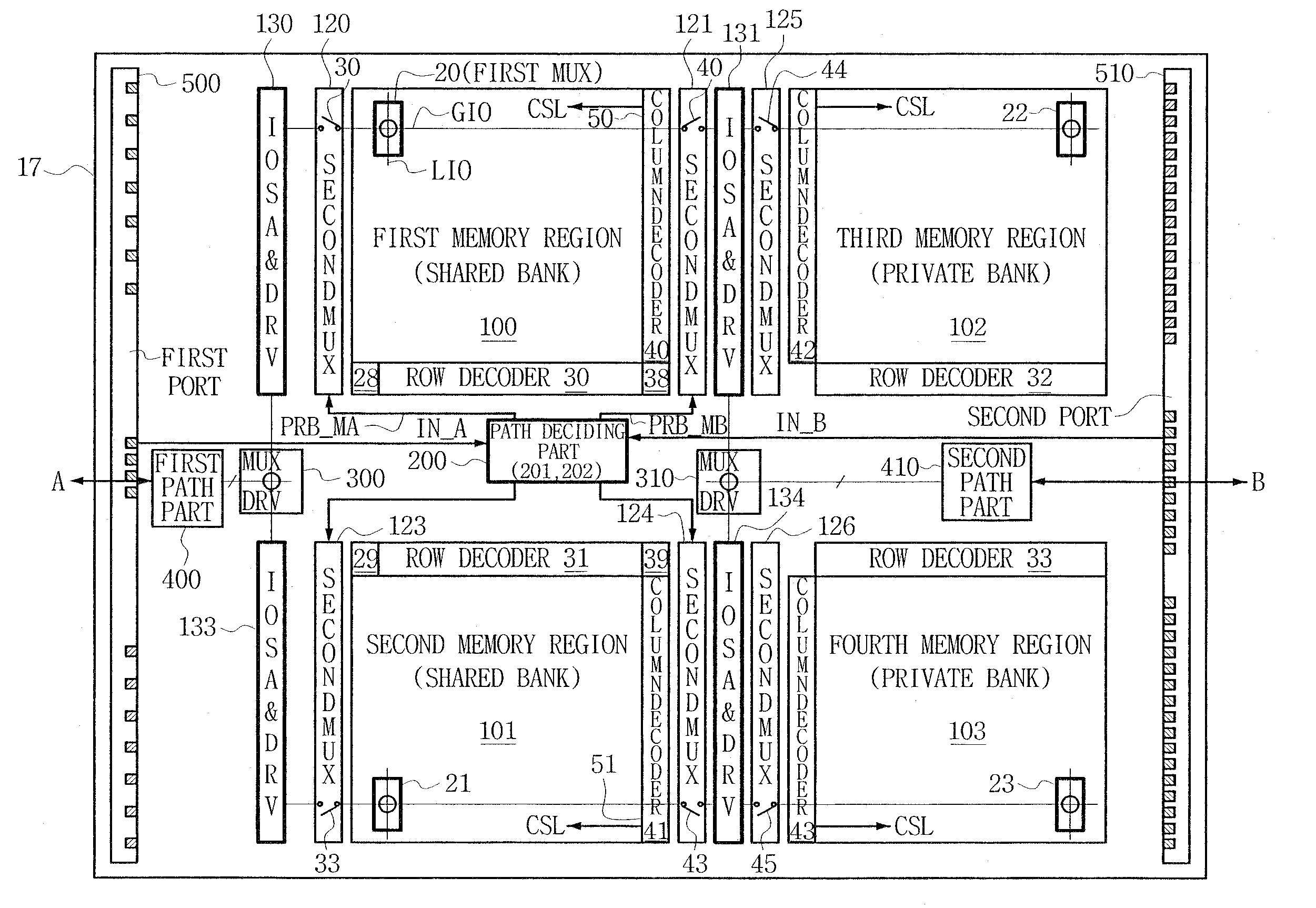
[0035]Embodiments are more fully described in detail with reference to FIGS. 5 to 15. However, embodiments many take different forms and should not be construed as being limited to the embodiments set forth herein. Rather, these embodiments are provided so that this disclosure is thorough and complete, and will enable one skilled in the art.

[0036]In the following description, other examples, published methods, procedures, general dynamic random access memory and circuits will not be described in detail so as not to obscure the embodiments.

[0037]In addition, although descriptive terms including letters such as A and B, and ordinal numbers such as first and second have been used, one skilled in the art will understand that the labeling is used solely to aid in discussion of the embodiments and not to imply an order, sequence, or number.

[0038]A multi-path accessible semiconductor memory device for use in a multi processor system according to embodiments will be described referring to t...


PUM


Abstract

A semiconductor memory device includes ports, data line pairs, where each port associated with one of the data line pairs, sets of address lines, where each port associated with one of the sets of address lines, a shared memory region of a memory cell array, where the shared memory region accessible through the ports, an access controller coupled to the ports and configured to generate an access selection signal in response to a plurality of control signals received through the ports, and an access router coupled to the shared memory region, the data line pairs, and the sets of address lines, the access router configured to selectively couple one of the sets of address lines and one of the data line pairs to the shared memory region in response to the access selection signal.

Description

CROSS-REFERENCE TO RELATED APPLICATIONS[0001]This application claims priority from Korean Patent Application No. 10-2005-127532, filed on 22 Dec. 2005, the content of which is incorporated by reference in its entirety for all purposes.BACKGROUND OF THE INVENTION[0002]1. Technical Field[0003]This disclosure relates to semiconductor memory devices, and more particularly, to multi-path accessible semiconductor memory devices for use in portable communication devices.[0004]2. Description of The Related Art[0005]In general, a semiconductor memory device having multiple access ports is called a multi port memory. In particular, a memory device having two access ports is called a dual port memory. A typical dual port memory, well known to those skilled in the field is an image processing video memory having a RAM (Random Access Memory) port to allow access in a random sequence and an SAM (Serial Access Memory) port to allow access only by a serial sequence.[0006]In order to differentiate a...

Claims


Application Information

Patent Timeline
Patent Type & Authority Applications(United States)
IPC IPC(8): G06F12/00
CPCG06F13/1663G11C7/1075G11C8/10G11C11/413G11C7/00G11C7/10G11C11/4096
Inventor KWON, KYOUNG-HWANSEO, DONG-ILLEE, HO-CHEOLSOHN, HAN-GUSHIN, YUN-HEE
Owner SAMSUNG ELECTRONICS CO LTD
Why Eureka
Try Eureka