Method for generating minimal leakage current input vector using heuristics

a leakage current input and input vector technology, applied in the field of integrated circuits, can solve the problems of severe power problem of devices, manual determination of predetermined input vectors, etc., and achieve the effect of reducing the leakage curren

Active Publication Date: 2007-06-28
IND TECH RES INST
View PDF12 Cites 7 Cited by
  • Summary
  • Abstract
  • Description
  • Claims
  • Application Information

AI Technical Summary

Benefits of technology

[0007] The present invention has been made to overcome the above-mentioned drawback of conventional leakage current reduction techniques. The pri...

Problems solved by technology

With the scaling down of integrated circuit (IC) design, the leakage current imposes severe power problem for devices with IC.
However, t...

Method used


Image

  • Method for generating minimal leakage current input vector using heuristics
  • Method for generating minimal leakage current input vector using heuristics
  • Method for generating minimal leakage current input vector using heuristics

Examples


Embodiment Construction

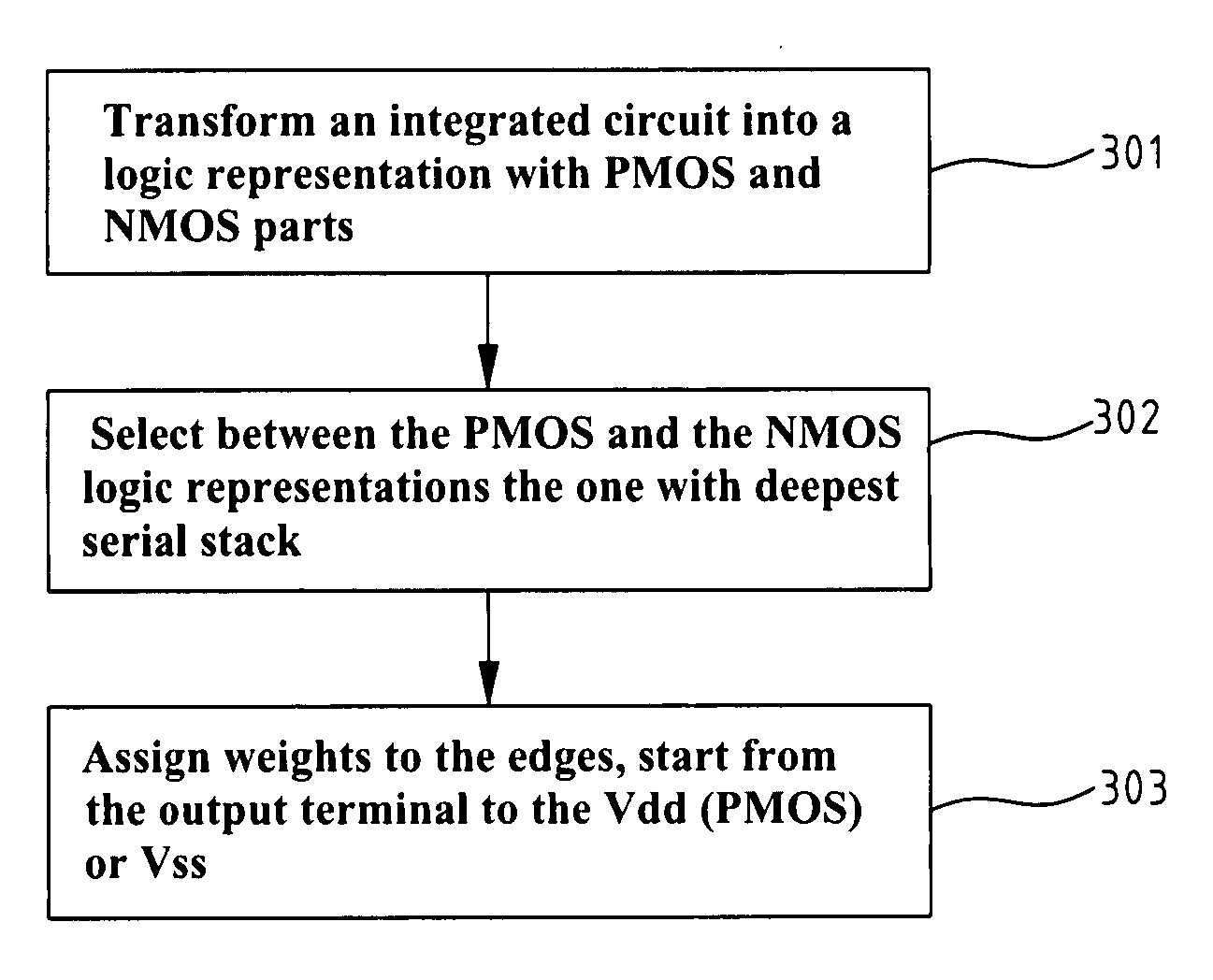
[0018]FIG. 3A shows a flowchart illustrating the method for generating input vector for minimizing the leakage current of the present invention. Referring to FIG. 3A, step 301 is to transform an integrated circuit, for example a CMOS circuit, into a logic representation with PMOS and NMOS parts. To more understand the operation of step 301, consider the following detailed description. For a given CMOS circuit, Vdd, Vss, output terminals and all wire connection points are transformed into nodes, and P and N devices of the given CMOS circuit are transformed into edges. To simplify the graph, only one node is used to represent connected edges. For example, if there are 10 devices directly connected to an output terminal, only one node is used to represent the output terminal. The transformed weighted graph is called WF, including two sub-graphs called, WFP (for PMOS) and WFN (for NMOS), respectively.

[0019] Step 302 in FIG. 3A is to select between the PMOS and the NMOS logic representa...


PUM


Abstract

A method for generating an input vector to reduce the leakage current in an integrated circuit by using heuristics includes transforming the integrated circuit to a logic representation with PMOS and NMOS parts and P and N devices of the integrated circuit into edges, selecting between PMOS and NMOS logic representations the one with deepest serial stack; and for the selected PMOS or NMOS logic representation, assigning weights to the edges, thereby generating a weighted graph. The assignment includes starting from the output terminal to the Power Vdd (for PMOS) or Ground Vss (for NMOS), and labeling edge weights in a descending order. The resulted cost function from the method of the present invention can be applied as heuristics in different algorithms, such as branch-and-bound, simulated annealing, or genetic algorithm.

Description

FIELD OF THE INVENTION [0001] The present invention generally relates to integrated circuits, and more specifically to a method for generating an input vector to reduce the leakage current in an integrated circuit by using heuristics. BACKGROUND OF THE INVENTION [0002] With the scaling down of integrated circuit (IC) design, the leakage current imposes severe power problem for devices with IC. The power consumed by an integrated circuit can be categorized as dynamic, static and current leakage, respectively. The leakage current consumes the power and generates heat even when the circuit is not in operation; hence, minimizing the leakage current can alleviate both the power consumption and the heat dissipation problems. [0003] U.S. Pat. No. 6,191,606 B1 (2001), “Method and apparatus for reducing standby leakage current using input vector activation” disclosed a method and an apparatus for reducing standby leakage current in CMOS circuit using selected input vectors. FIG. 1 shows the ...

Claims


Application Information

Patent Timeline
IPC IPC(8): G06F17/50
CPCG01R31/3008G06F17/504G06F30/3323
Inventor SU, PEISHENG ALANWENG, LI-CHUAN
Owner IND TECH RES INST
Why Eureka
Try Eureka