Nanowire structures and devices for use in large-area electronics and methods of making the same

a technology of nanowires and electronics, applied in nanoinformatics, magnetic materials, magnetic bodies, etc., can solve the problems of limited device performance, difficult plastic substrate fabrication of transistors such as field effect transistors (fets) or thin film transistors (tfts) and the inability to integrate these devices over large area substrates

Inactive Publication Date: 2007-07-05
MOMENTIVE PERFORMANCE MATERIALS INC
View PDF12 Cites 104 Cited by
  • Summary
  • Abstract
  • Description
  • Claims
  • Application Information

AI Technical Summary

Problems solved by technology

Although rapid miniaturization of microelectronics has led to cost reduction, integration of these devices over large area substrates still poses challenges in terms of device efficiency and reliability.
Current large-area and low-cost electronic devices are primarily based on amorphous silicon (a-Si) or polycrystalline silicon (poly-Si) transistors on glass, and the device performance is limited due to low carrier mobilities in amorphous silicon (a-Si) or poly-Si.
However, the fabrication of transistors such as field effect transistors (FETs) or thin film transistors (TFTs)

Method used


Image

  • Nanowire structures and devices for use in large-area electronics and methods of making the same
  • Nanowire structures and devices for use in large-area electronics and methods of making the same
  • Nanowire structures and devices for use in large-area electronics and methods of making the same

Examples


Embodiment Construction

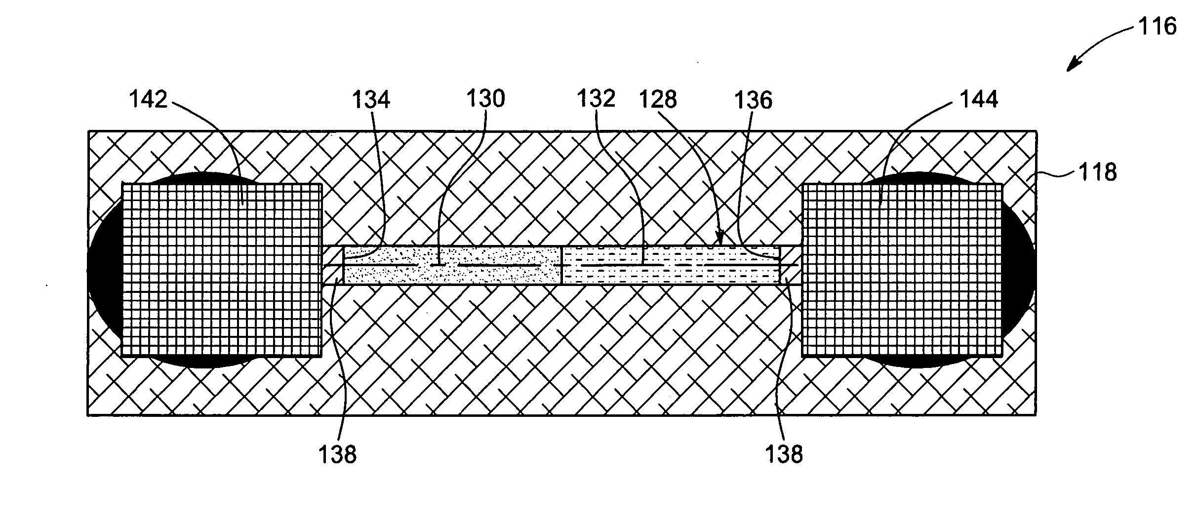
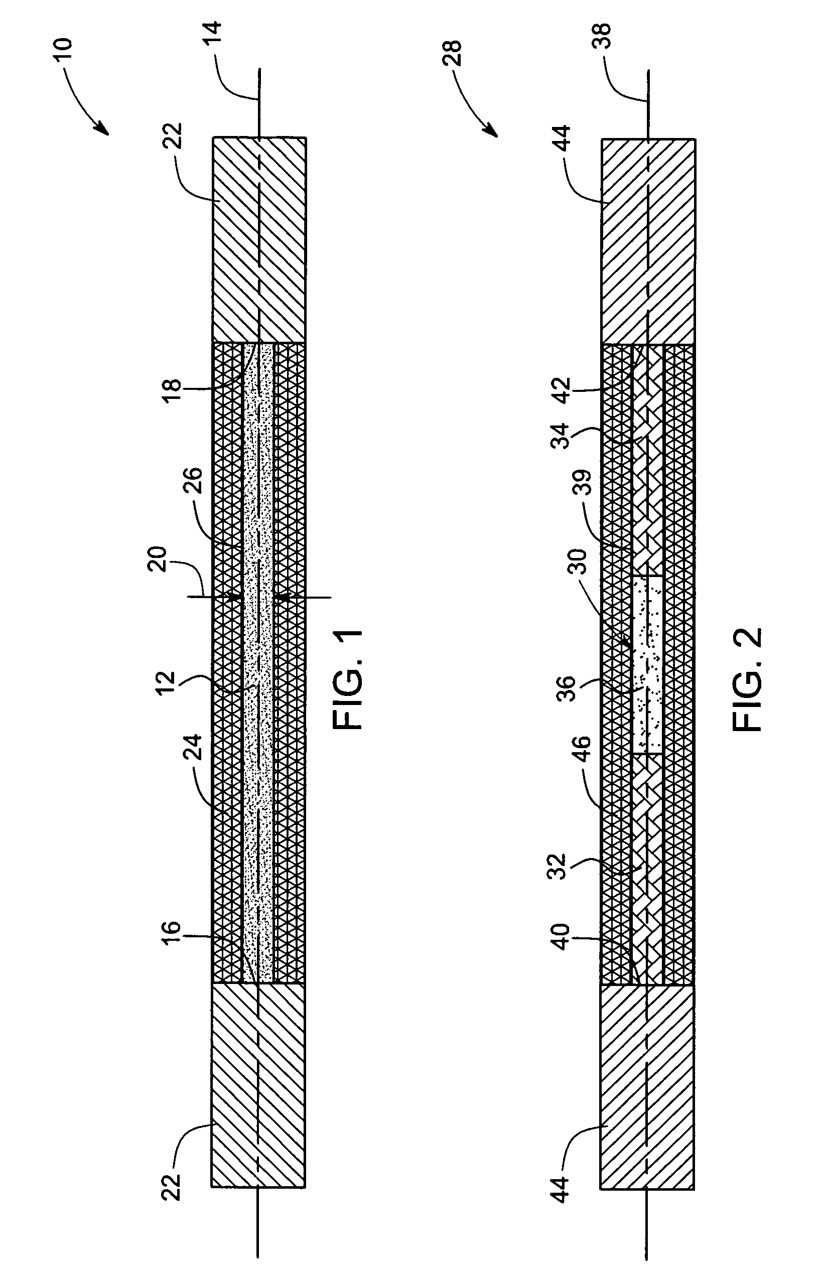
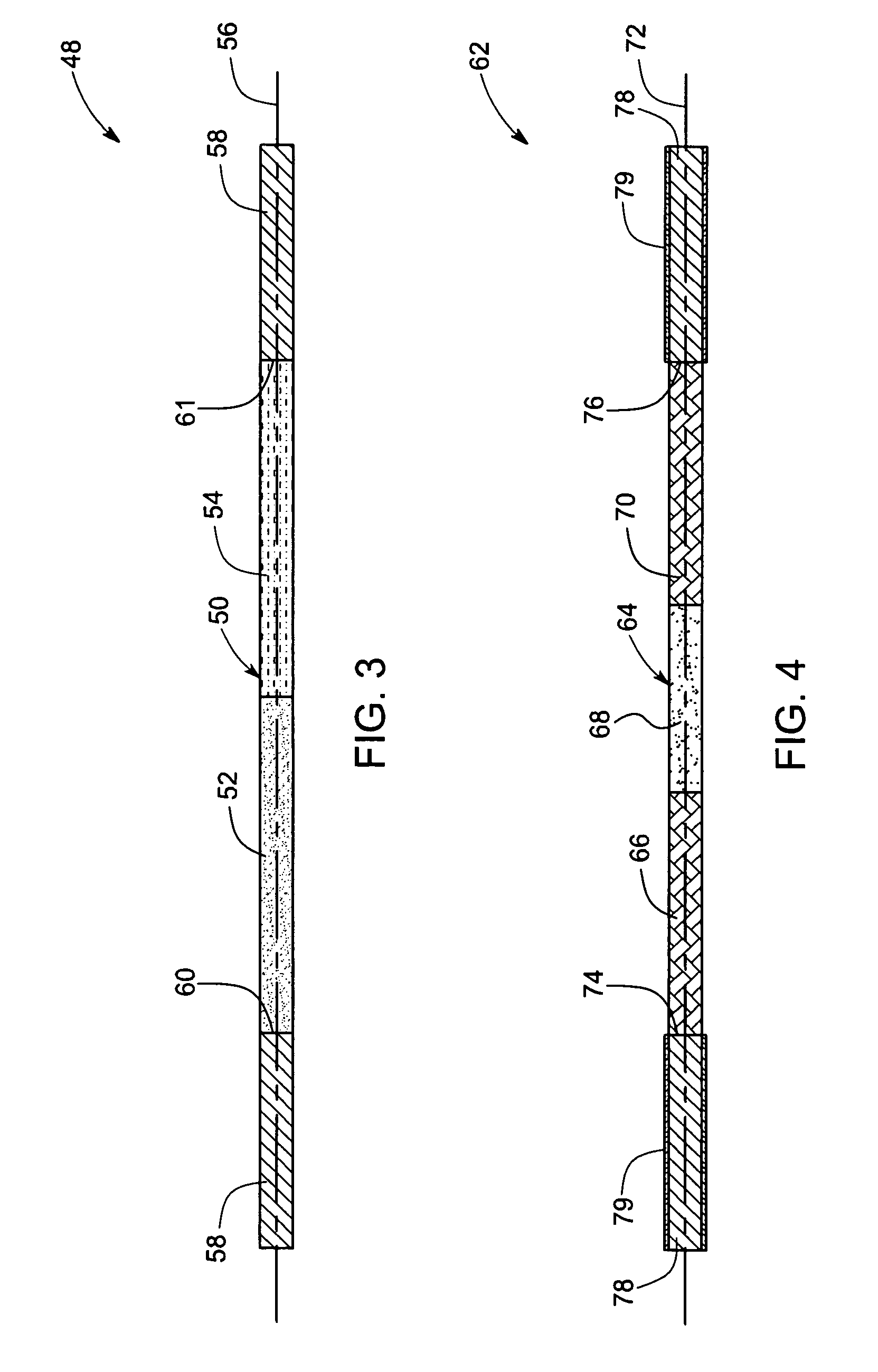
[0023] Nanowires made of materials, such as semiconductors or inorganic materials, are being used in large area electronic devices to improve the performance of the devices. Also, the nanowires are being used in conventional electronic devices to achieve improved device behavior, while allowing for inexpensive and fast manufacturing processes. The semiconductor nanowires are single-crystal and have comparable or better electron or hole mobility than their corresponding bulk forms. These nanowires are mostly employed in the form of films of semiconductor materials, which may be used in electronic devices to make high performance, low cost devices on large and flexible substrates. In order to effectively employ such nanowires in electronics devices, it is desirable to form low-resistance and reliable electrical contacts to these nanowire in a manufacturable fashion. As used herein, “manufacturable” implies that the electrical contacts may be made at a high rate in a scaleable process ...


PUM


Abstract

A nanowire structure and device for use in large area electronics and methods of making the same is provided. The nanowire structure includes a nanowire defining an axis, where the nanowire includes a first end and a second end. The first end is axially spaced from the second end. Further, the nanowire structure includes magnetic segments that are coupled to the first and second ends of the nanowire.

Description

BACKGROUND [0001] The invention relates generally to the field of large-area electronics on flexible or rigid substrate, and more particularly to the large-area flexible electronics enabled by nanowire structures and methods of making the same. [0002] Although rapid miniaturization of microelectronics has led to cost reduction, integration of these devices over large area substrates still poses challenges in terms of device efficiency and reliability. Current large-area and low-cost electronic devices are primarily based on amorphous silicon (a-Si) or polycrystalline silicon (poly-Si) transistors on glass, and the device performance is limited due to low carrier mobilities in amorphous silicon (a-Si) or poly-Si. These transistors are being used in various applications, such as flat panel displays (FPDs), solar cells, image sensor arrays and digital X-ray imagers. [0003] There has been growing interest in the use of plastic as a substrate for large-area electronics due to various ben...

Claims


Application Information

Patent Timeline
IPC IPC(8): H01L21/36
CPCB82Y10/00H01F1/405B82Y40/00H01F1/0072H01F1/009H01F41/30H01L29/0665H01L29/0673H01L29/0676H01L29/068H01L29/16H01L29/20H01L29/22H01L29/24H01L29/772H01L33/18H01L2924/0002B82Y25/00H01L2924/00
Inventor ZHANG, ANPINGLI, YUNFEIST, THOMAS PAULHUBER, WILLIAM HULLINGER
Owner MOMENTIVE PERFORMANCE MATERIALS INC
Why Eureka
Try Eureka