Combination of a substrate and a wafer

Active Publication Date: 2007-07-05
THALLNER ERICH
View PDF4 Cites 50 Cited by
  • Summary
  • Abstract
  • Description
  • Claims
  • Application Information

AI Technical Summary

Benefits of technology

[0009]The invention is based on the objective of proposing a combination of a substrate and a wafer, in which the connection between the substrate and the wafer withstands the temperatures occurring during a rethinning process without damages and can be separated with si

Problems solved by technology

If silicone is used as the base material for the electric circuits, a silicon wafer is also used as the substrate in practical applications due to the favorable costs and the identical coefficient of thermal expansion.
The adhesive used has the peculiar property of losing its adhesive properties once a certain temperature is exceeded.
The disadvantage of this known method in practical applications can be seen in that the adhesive frequently is already destroyed by the temperatures occurring during the rethinning process such that the wafer already separates from its substrate during th

Method used


Image

  • Combination of a substrate and a wafer
  • Combination of a substrate and a wafer
  • Combination of a substrate and a wafer

Examples


Example

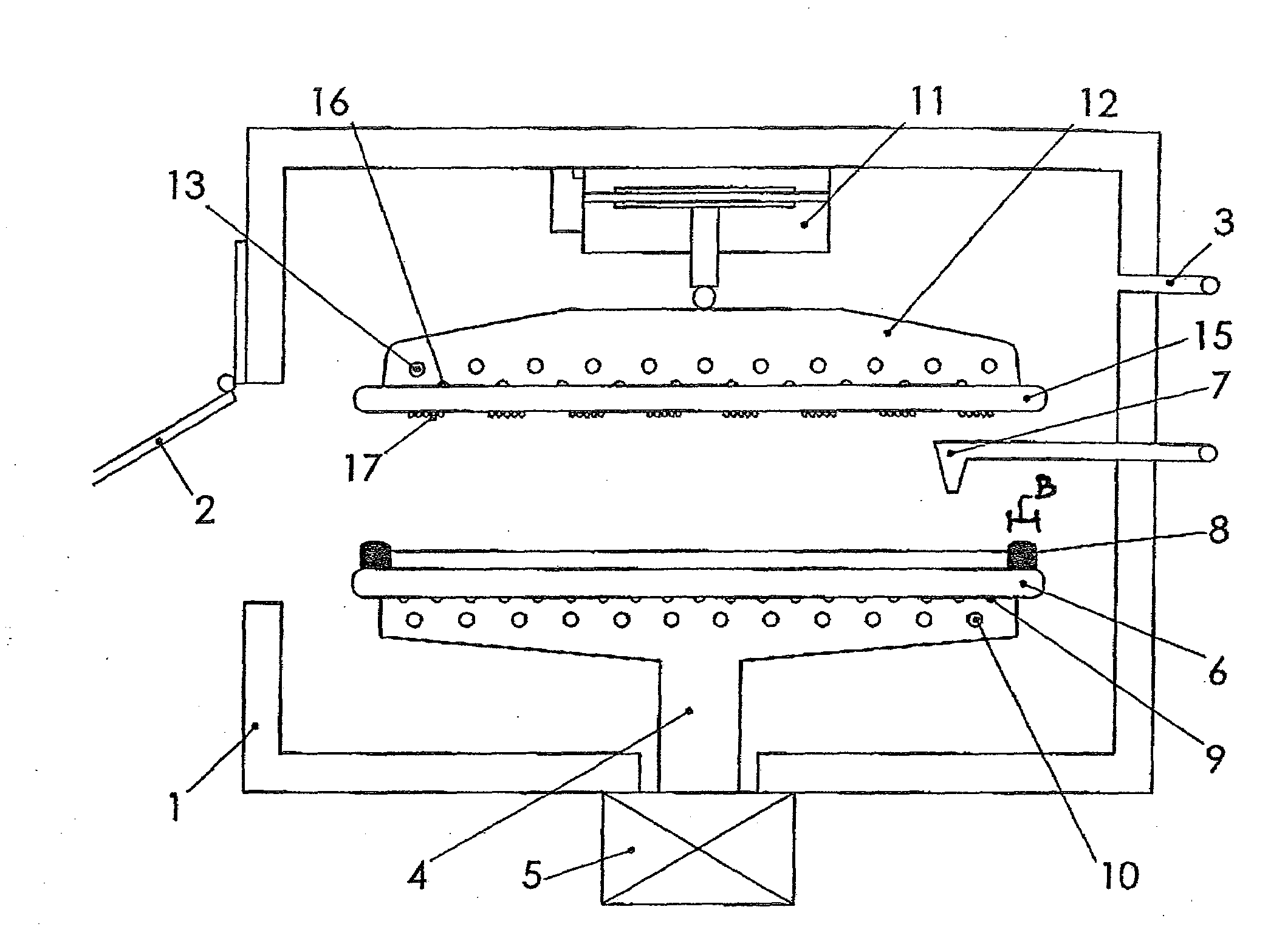
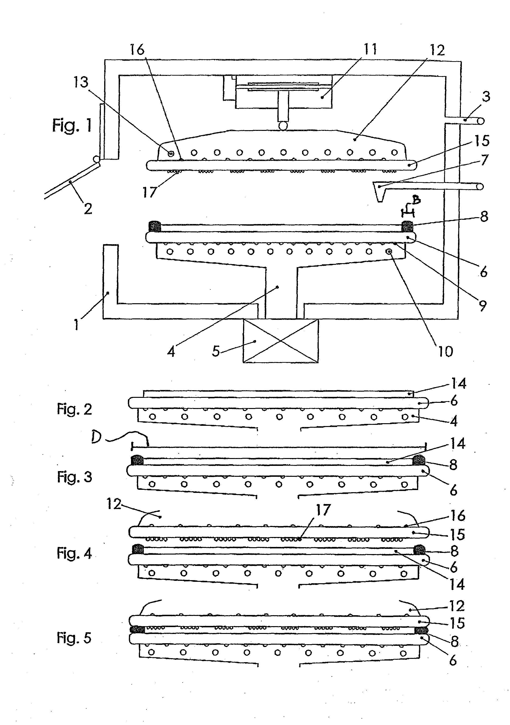
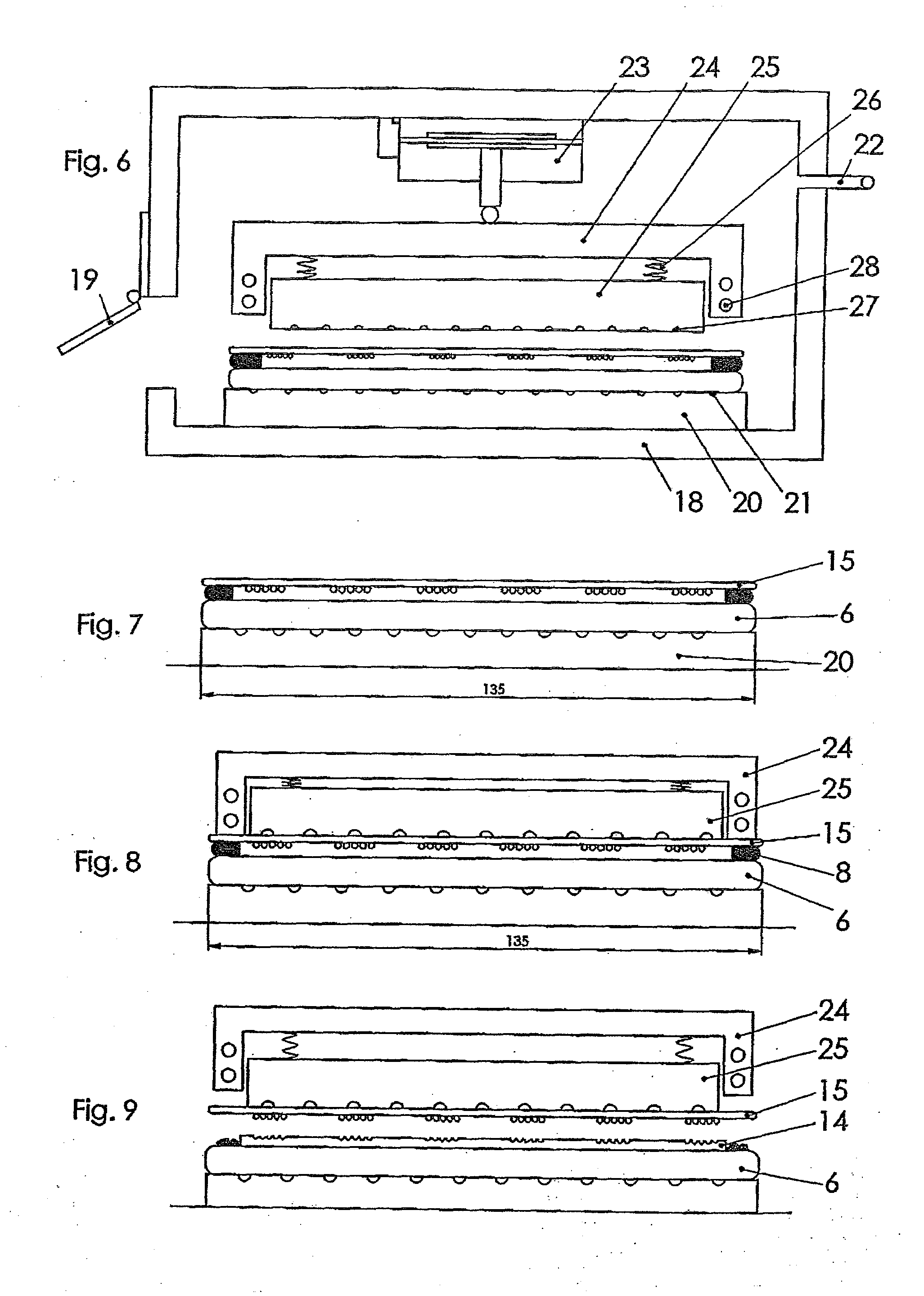
[0034]In the figures, identical components and components with identical functions are identified by the same reference symbol.

[0035]FIG. 1 shows a device for connecting a wafer 15 with a substrate 6. The device comprises a chamber 1 with a cover 2. The cover 2 serves for tightly closing the chamber 1 relative to the surroundings. The cover 2 simultaneously serves for loading the chamber 1 with the substrate 6 and the wafer 15. The chamber 1 can be evacuated by means of a not-shown vacuum pump and a vacuum line 3 so as to prevent air inclusions when the connection between the substrate 6 and the wafer 15 is produced.

[0036]A receptacle device 4 (chuck) for accommodating the substrate 6 is provided within the chamber 1. The receptacle device is connected to a motor unit 5. The receptacle device 4 can be set in rotation by means of the motor unit 5.

[0037]The device furthermore comprises an adjustable nozzle 7 for applying the fluid adhesive on the substrate 6. Suitable adhesives are ba...


PUM


Abstract

The invention pertains to a combination of a substrate (6) and a wafer (15), wherein the substrate (6) and the wafer (15) are arranged parallel to one another and bonded together with the aid of an adhesive layer (8) situated between the substrate (6) and the wafer (15), and wherein the adhesive is chosen such that its adhesive properties are neutralized or at least diminished when a predetermined temperature is exceeded. According to the invention, the adhesive layer (8) is only applied annularly between the substrate (6) and the wafer (15) in the edge region of the wafer (15).

Description

FIELD OF THE INVENTION [0001]The invention pertains to a combination of a substrate and a wafer, a device for separating a combination of a wafer and a substrate as well as a method for handling a substrate and a wafer.BACKGROUND OF THE INVENTION [0002]In the semiconductor industry, it is necessary to subject a wafer to a rethinning process after its structuring in order to reduce the axial or vertical dimensions and to realize electrical and thermal improvements of the finished product. In the rethinning process, the non-structured side of the wafer is removed by means of mechanical grinding methods. The electrically active layer and, if applicable, any contacting terminals provided on the wafer surface that are usually realized in the form of small soldering globules (pumps) remain untouched.[0003]Since the rethinning process is usually realized by grinding the wafer mechanically as mentioned above, it is necessary to fix the wafer on a stable substrate in order to stabilize the w...

Claims


Application Information

Patent Timeline
IPC IPC(8): H01L21/30
CPCH01L21/67092Y10T156/11H01L2221/68318H01L2221/6834H01L21/02002H01L21/2007H01L2924/01076H01L21/6838Y10T156/17Y10T156/19Y10T428/26Y10T156/1361Y10T156/10Y10T156/1798Y10T428/24331H01L21/6835Y10T428/31511
Inventor THALLNER, ERICH
Owner THALLNER ERICH
Why Eureka
Try Eureka