Method and computer program product for trimming the analysis of physical layout versus schematic design comparison

a technology of physical layout and schematic design, applied in the field of microelectronic integrated circuits, can solve the problems of time and resources, layout design is not practical without the aid of computers, and unintentional circuit structure extraction adds bulk and complexity to the layout netlist,

Inactive Publication Date: 2007-07-05
BELL SEMICON LLC
View PDF7 Cites 40 Cited by
  • Summary
  • Abstract
  • Description
  • Claims
  • Application Information

AI Technical Summary

Problems solved by technology

These blocks are ones that have proven quality and so their implementation saves time and resources.
Due to the large number of components and the exacting details required by the fabrication process, layout design is not practical without the aid of computers.
However, if the unintentional circuit structure has been resolved in previous iterations of the integrated circuit verification, the unintentional circuit structure extraction add bulk and complexity to the layout netlist.
Any additional bulk and complexity in the layout netlist extracted translates into a longer and more complex Layout Versus Schematic Error Report.

Method used


Image

  • Method and computer program product for trimming the analysis of physical layout versus schematic design comparison
  • Method and computer program product for trimming the analysis of physical layout versus schematic design comparison
  • Method and computer program product for trimming the analysis of physical layout versus schematic design comparison

Examples


Embodiment Construction

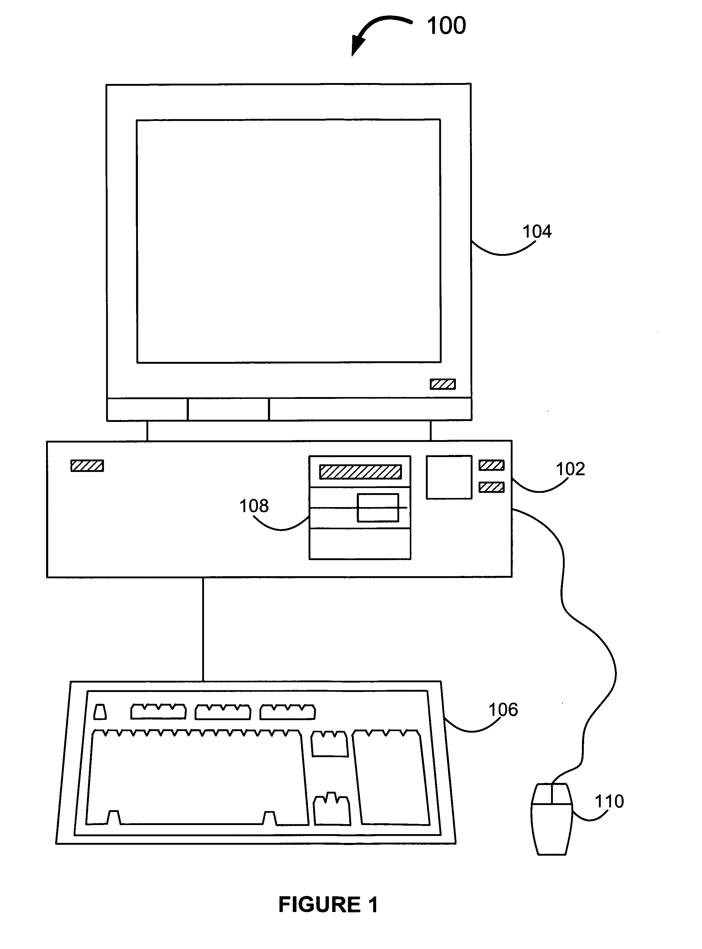
[0028] With reference now to the figures and in particular with reference to FIG. 1, a pictorial representation of a data processing system in which the aspects of the present invention may be implemented. A computer 100 is depicted which includes system unit 102, video display terminal 104, keyboard 106, storage devices 108, which may include floppy drives and other types of permanent and removable storage media, and mouse 110. Additional input devices may be included with personal computer 100, such as, for example, a joystick, touchpad, touch screen, trackball, microphone, and the like. Computer 100 can be implemented using any suitable computer, such as an IBM eServer computer or IntelliStation computer, which are products of International Business Machines Corporation, located in Armonk, N.Y. Although the depicted representation shows a computer, other embodiments of the present invention may be implemented in other types of data processing systems, such as a network computer. ...


PUM


Abstract

A method, a computer program product, and an apparatus for performing a trimmed verification analysis comprising selecting layers of interest for a trimmed analysis, eliminating layer definitions for unselected layers to create a trimmed rundeck, and performing a layout versus schematic verification comparison to generate a trimmed error report for the selected layers of interest.

Description

BACKGROUND OF THE INVENTION [0001] 1. Technical Field [0002] The present invention relates generally to microelectronic integrated circuits. In particular, the present invention relates to a method, computer program product, and an apparatus for reducing turn-around-time in the physical design layout, routing and verification cycle of a microelectronic integrated circuit. [0003] 2. Description of the Related Art [0004] Microelectronic integrated circuits (ICs) are fabricated by layering several different materials on a semiconductor wafer. The typical integrated circuit is formed from dozens of layers. These layers can be formed by depositing material on the integrated circuit such as metal and poly, growing material on the integrated circuit such as oxides, or doping areas of the integrated circuit with different impurities. [0005] The design of the integrated circuit is a two part process. First, integrated circuits are functionally designed in a schematic circuit format. Secondly...

Claims


Application Information

Patent Timeline
Patent Type & Authority Applications(United States)
IPC IPC(8): G06F17/50
CPCG06F17/5081G06F30/398
Inventor HOLESOVSKY, ALAN LEELAKSHMANAN, VISWANATHANACOTT, BRENT WRAY
Owner BELL SEMICON LLC
Why Eureka
Try Eureka