Silicon wafer, method for manufacturing the same and method for growing silicon single crystals

a technology of silicon single crystals and silicon wafers, which is applied in the direction of silicon compounds, silicates, and under a protective fluid, can solve the problems of harmful grown-in defects, deleterious effects on device characteristics, and affecting device manufacturing, etc., and achieves a wide range of pull rate, easy growth, and higher pull rate

Active Publication Date: 2007-07-12
SUMCO CORP
View PDF3 Cites 9 Cited by
  • Summary
  • Abstract
  • Description
  • Claims
  • Application Information

AI Technical Summary

Benefits of technology

[0021] It is therefore an object of the invention to provide a method for growing silicon single crystals by which grown-in defect-free crystals, particularly crystals consisting essentially of a PI region, can be manufactured stably and efficiently. Additional objects of the invention are to provide high-quality and low-cost mirror-polished silicon wafers prepared with the aid of such a method for growing silicon single crystals, and to provide a method for manufacturing such silicon wafers.

Problems solved by technology

In a silicon single crystal produced in this way, various grown-in defects are known to be formed which cause problems during device fabrication.
Both dislocation clusters and COPs are harmful grown-in defects that have deleterious effects on device characteristics.
However, with the rapid trend in integrated circuits towards smaller geometries in recent years, even the harmfulness of COPs has become of concern.

Method used


Image

  • Silicon wafer, method for manufacturing the same and method for growing silicon single crystals
  • Silicon wafer, method for manufacturing the same and method for growing silicon single crystals
  • Silicon wafer, method for manufacturing the same and method for growing silicon single crystals

Examples


examples

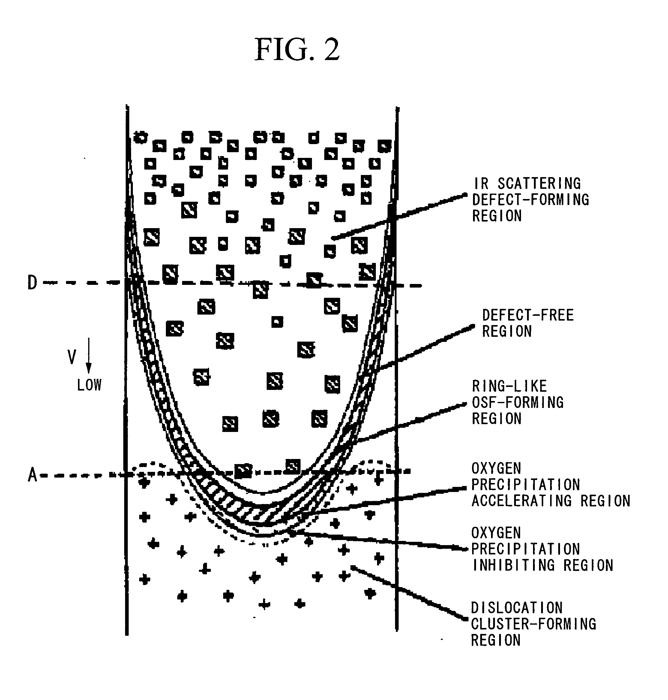
[0125] To verify the advantageous effects of the present invention, crystals were pulled under conditions that the pull rate was varied in a V-shaped manner and an apparatus for growing silicon single crystals with a 16-inch quartz crucible capable of growing a 6-inch crystal was used. The distribution of grown-in defects was evaluated.

[0126] The pull rate was varied, in terms of the ratio to the maximum pull rate, from 0.7 to 0.35 to 0.7. The hydrogen concentrations and pressures within the furnace during pulling were set respectively to (a) 0% and 4.0 kPa (30 torr), (b) 6% and 4.0 kPa (30 torr), and (c) 6% and 9.3 kPa (70 torr). Each of the resulting pulled crystals was vertically sectioned along the crystal axis, and the defect distribution within the resulting section was examined.

[0127] The results are shown in FIG. 11. The sectioned surfaces were treated as follows.

[0128] The single crystals that have been grown in this way under different hydrogen concentrations were verti...


PUM

PropertyMeasurementUnit
diameteraaaaaaaaaa
diameteraaaaaaaaaa
temperatureaaaaaaaaaa

Abstract

This silicon wafer is obtained from a silicon single crystal grown by the CZ method in a hydrogen-containing inert gas atmosphere, and is a completely grown-in defect-free wafer containing no COPs or dislocation clusters throughout the wafer in the thickness and radial directions thereof, and all the portions consist essentially of an interstitial rich region. This method for growing silicon single crystals includes pulling a silicon single crystal in a hydrogen-containing inert gas atmosphere so as to expand the range of the pull rate for the PI region, wherein the pulling of the silicon single crystal is conducted at a pull rate within this expanded range of the pull rate for the PI region so as to grow a body portion that is an interstitial rich region.

Description

[0001] TECHNICAL FIELD [0002] The present invention relates to silicon wafers and a method for manufacturing the same, from which semiconductor devices can be fabricated, and also relates to a method for growing silicon single crystals from which silicon wafers can be prepared. More particularly, the present invention relates to techniques suitable for use in the preparation of what are known as grown-in defect-free wafers. [0003] This application claims priority from Japanese Patent Application No. 2004-246017, filed on Aug. 25, 2004, Japanese Patent Application No. 2005-163152, filed on Jun 2, 2005, and Japanese Patent Application No. 2005-239529, filed on Aug. 22, 2005, the contents of which are incorporated herein by reference. BACKGROUND ART [0004] The rotational pulling process known as the Czochralski (CZ) method is representative of the methods for manufacturing silicon single crystals used to prepare silicon wafers. In the production of a silicon single crystal by the CZ me...

Claims


Application Information

Patent Timeline
Patent Type & Authority Applications(United States)
IPC IPC(8): C30B15/00C30B21/06
CPCC30B15/04C30B29/06C30B15/203C30B15/20
Inventor HOURAI, MASATAKASUGIMURA, WATARUONO, TOSHIAKI
Owner SUMCO CORP
Why Eureka
Try Eureka