Groove composite multi-bulge structure and preparation process thereof
A technology for preparation process and recessed structure, which is applied in the direction of microstructure technology, microstructure device, manufacturing microstructure device, etc., can solve the problems of poor repeatability and high cost of the preparation process, and achieve improved SERS activity, light absorption capacity, Improving the effect of enhancers
- Summary
- Abstract
- Description
- Claims
- Application Information
AI Technical Summary
Problems solved by technology
Method used
Image
Examples
Embodiment 1
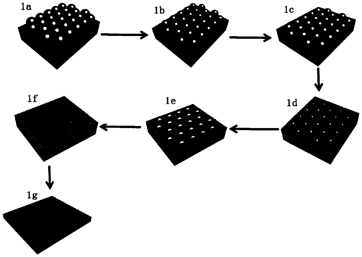
[0044] Example 1 - Fabrication of Groove Composite Multi-Protrusion Structure by Reactive Ion Etching Process
[0045] Step 1. Forming a silicon-based groove array structure
[0046] Step 1a, put the silicon wafer into deionized water, acetone, ethanol, concentrated sulfuric acid, hydrogen peroxide, and deionized water in sequence for ultrasonic cleaning, each liquid is ultrasonically cleaned for 30-40 minutes, and then the cleaned silicon wafer is dried at 120°C For treatment, the drying time is 20 minutes; after the water on the silicon wafer is completely evaporated, the silicon wafer is placed in an ultraviolet ozone cleaning machine for 30 minutes of irradiation to obtain a silicon wafer with a hydrophilic surface. Take 30 microliters of PS colloidal sphere suspension with a content of 2.5wt% and a diameter of 100 nm, mix it with ethanol in an equal volume, and then perform ultrasonic oscillation for 10 to 30 minutes, so as to obtain a uniformly dispersed ethanol dilution...
Embodiment 2
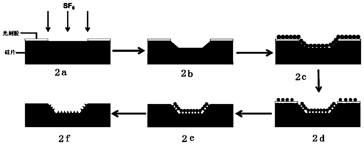
[0053] Example 2 - Preparation of groove composite multi-protrusion structure by photolithography technology combined with reactive ion etching process
[0054] The specific operation process of the photolithography process is in the prior art, and will not be repeated here. Due to the limitation of the lithography precision of the lithography instrument, the interval period width of the lithography mask plate during lithography is 10um. After constructing grooves with a width of 10 μm through the existing photolithography technology and reactive ion etching process, a 100 nm PS ball array was prepared by the same method as in step 1a of Example 1, and the above-mentioned obtained width of The 10um silicon-based groove array structure is compounded. After the above-mentioned silicon plate is naturally air-dried, the 100nm PS ball array is used as a secondary mask layer, and then the same process parameters as in the second etching of Example 1 are used for reactive ion etching...
Embodiment 3
[0055] Example 3 - Fabrication of Groove Composite Multi-Protrusion Structure by Reactive Ion Etching Process
[0056] Step 1. Forming a silicon-based groove array structure
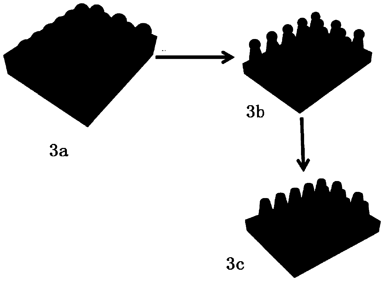
[0057] Step 1a, using the same method as step 1a in Example 1, respectively obtain a 100nm single-layer ordered hexagonal close-packed PS sphere array and a 500nm single-layer ordered hexagonal close-packed PS sphere array, such as Figure 6 Shown in a.
[0058] Step 1b, performing plasma etching on the 500nm single-layer ordered hexagonal close-packed PS sphere array prepared in step 1a, using oxygen as the working gas, controlling the gas flow at 30 sccm, maintaining the gas pressure at 3Pa, and controlling the etching power at 200W, and the total etching time is 40s at high-end or 3min at mid-range, so as to obtain a non-hexagonal close-packed PS ball array structure with a surface size of 350nm-450nm on the silicon wafer, such as Figure 6 Shown in b.
[0059] Step 1c, using the non-hexagonal clos...
PUM
| Property | Measurement | Unit |
|---|---|---|
| size | aaaaa | aaaaa |
| diameter | aaaaa | aaaaa |
| thickness | aaaaa | aaaaa |
Abstract
Description
Claims
Application Information


