Display Device and Production Method Thereof

Inactive Publication Date: 2007-07-12
HITACHI DISPLAYS
View PDF13 Cites 42 Cited by
  • Summary
  • Abstract
  • Description
  • Claims
  • Application Information

AI Technical Summary

Benefits of technology

[0011] Bonding glass which easily crystallizes and which is readily used for the present invention described above has a composition of, for example, V2O5: 55 to 60 wt %, P2O5: 20 to 25 wt %, BaO: 5 to 10 wt %, Sb2O3: 5 to 10 wt %, TeO2: 0 to 5 wt %, WO3: 0 to 5 wt %, and ZnO: 0 to 5 wt % in oxide conversion. For glass which will not easily crystallize, the precipitation of a crystalli

Problems solved by technology

However, if this drawing of the adhesive layer occurred, the adhesive layer will not remain sufficiently in the adhesion surface and thus a required adhesive str

Method used


Image

  • Display Device and Production Method Thereof
  • Display Device and Production Method Thereof
  • Display Device and Production Method Thereof

Examples


example 1

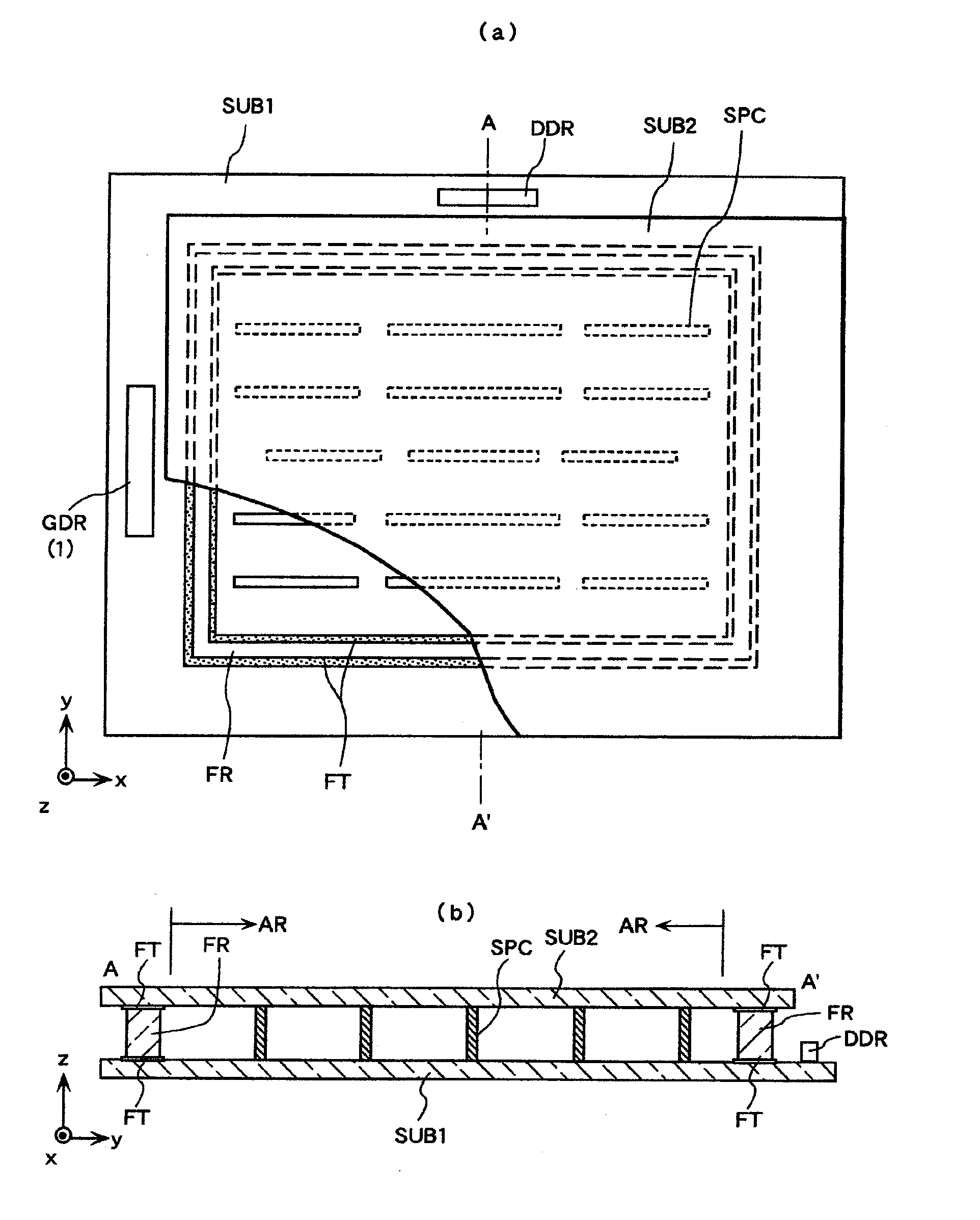
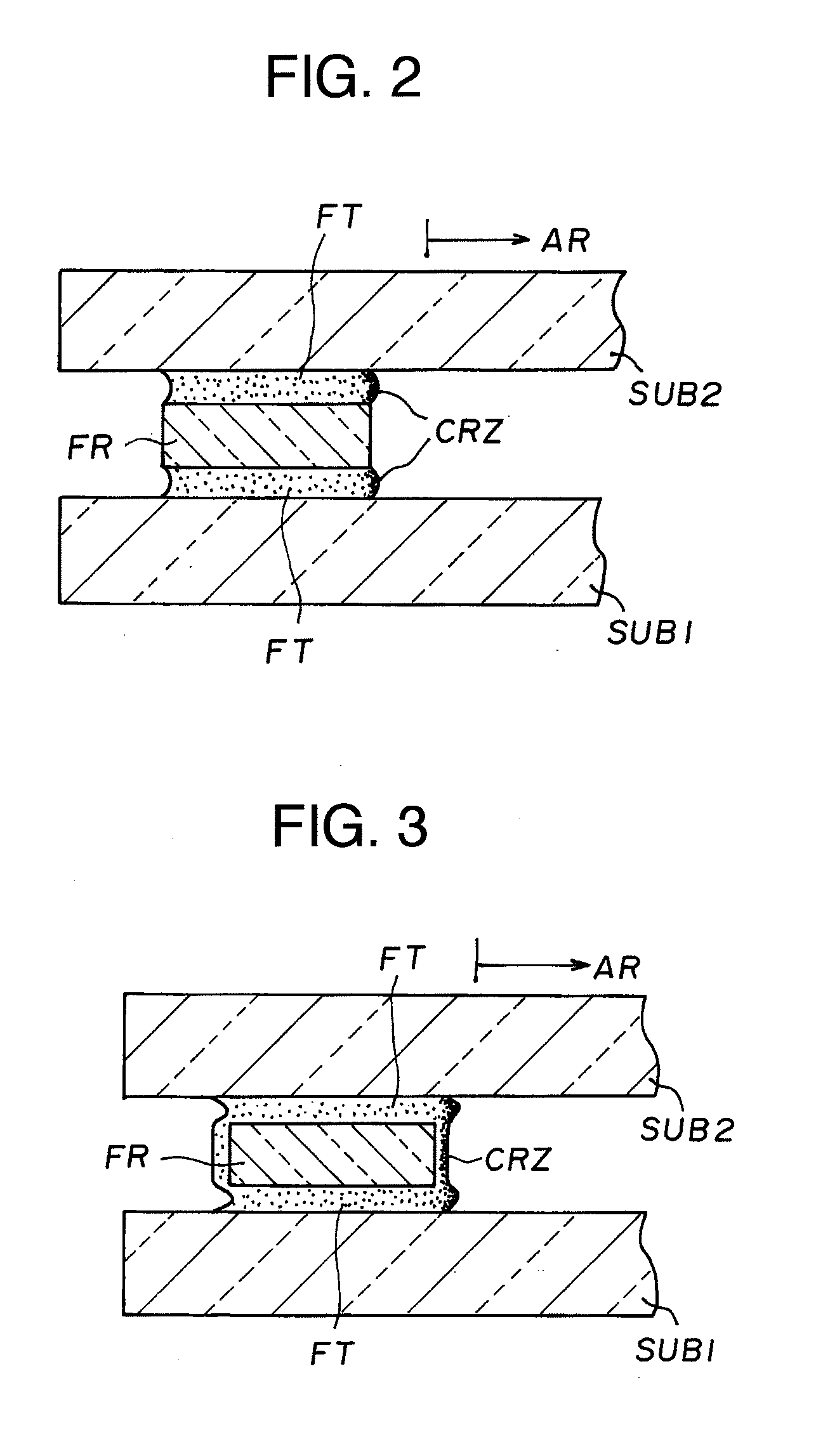
[0034]FIG. 2 is a cross sectional view of a principal part explaining Example 1 of a display device according to the present invention. In FIG. 2, the adhesive layer FT is applied to between the respective contact surfaces of the first glass substrate SUB1 and sealing frame FR, as well as of the second glass substrate SUB2 and sealing frame FR. In Example 1, a crystalline layer CRZ is provided in the surface of the adhesive layer FT facing to the interior on a display region AR side. The layer thickness of this crystalline layer CRZ is approximately 10 μm.

[0035] The assembly is carried out so that the first glass substrate SUB1, the second glass substrate SUB2, and the sealing frame FR may provide an airtight container. In this airtight container, the sealing frame FR to which the adhesive layer FT is applied is interposed between the first glass substrate SUB1 and the second glass substrate SUB2, and the interior on the display region AR side is vacuum pumped while heating. Nonlea...

example 2

[0039]FIG. 3 is a cross sectional view of a principal part explaining Example 2 of a display device according to the present invention. In FIG. 3, the adhesive layer FT is applied to the whole surface including between the respective contact surfaces of the first glass substrate SUB1 and the sealing frame FR, as well as of the second glass substrate SUB2 and the sealing frame FR, and the side surfaces. In Example 2, the crystalline layer CRZ is provided in the surface of the adhesive layer FT facing to the interior on the display region AR side. Other structures are the same as those of Example 1. Then, the processes of heating, reheating, and vacuum pumping the airtight container are the same as those of Example 1.

[0040] Then, also in Example 2, in the first heating, the crystalline layer may be formed also in the outer surface of the adhesive layer FT by making the atmosphere of the whole interior of the baking furnace reductive. Accordingly, a decrease in adhesive strength due t...

example 3

[0041]FIG. 4 is a cross sectional view of a principal part explaining Example 3 of a display device according to the present invention. In Example 3, the crystalline layer CRZ is formed in the surface of the adhesive layer FT of the sealing frame FR except each contact surface of the first glass substrate SUB1 and the sealing frame FR, as well as of the second glass substrate SUB2 and the sealing frame FR. This example is a structure suitable for display devices designed to seal a gas inside the airtight container, e.g., a plasma display device.

[0042] That is, Example 3 is suitable for sealing in the case where the interior of the airtight container is not in a highly low-pressure atmosphere like the vacuum state of Example 1 or Example 2. For this reason, although it is not necessary to interpose the adhesive layer FT between the respective contact surfaces of the first glass substrate SUB1 and sealing frame FR, as well as of the second glass substrate SUB2 and sealing frame FR, i...


PUM

PropertyMeasurementUnit
Percent by volumeaaaaaaaaaa
Volumeaaaaaaaaaa
Adhesion strengthaaaaaaaaaa

Abstract

An object of the present invention is to provide a highly reliable display device by preventing an adhesive layer from being drawn to the inside at the time of vacuum pumping and by securing a sufficient adhesive strength. A crystalline layer CRZ is formed in the surface of an adhesive layer FT between the respective contact surfaces of a first glass substrate SUB1 and a sealing frame FR, as well as of a second glass substrate SUB2 and the sealing frame FR.

Description

FIELD OF THE INVENTION [0001] The present invention relates to display devices and production methods thereof, and is suitable in particular for flat panel type display devices whose interior is an airtight container. BACKGROUND OF THE INVENTION [0002] As display devices excellent in high brightness and high definition, liquid crystal display devices, plasma display devices, and the like are put in practical use in place of conventional color cathode ray tubes. Moreover, among others, as those allowing for higher brightness, various types of panel type display devices such as an electron emission type display device, an organic electroluminescence display device characterized in low power dissipation, and the like, are put in practical use or are in preliminary stages for practical use. [0003] Patent documents related to the electron emission type display device include Patent Document 1 (JP-A-9-283059), Patent Document 2 (JP-A-2000-21335), Patent Document 3 (JP-A-8-22782), etc. In ...

Claims


Application Information

Patent Timeline
IPC IPC(8): B29C65/00
CPCH01J5/20H01J9/261Y10T428/10H01J2209/264H01J31/123C03C3/122C03C3/16C03C8/04C03C8/08C03C8/24C03C27/10C09K2323/00
Inventor SAWAI, YUICHISHIONO, OSAMUNAMEKAWA, TAKASHIAKATA, HIROYUKINAITO, TAKASHIKANAZAWA, KEIICHIKIJIMA, YUUICHIHIRASAWA, SHIGEMIASAKURA, SHUNICHIHAYASHIBARA, MITSUO
Owner HITACHI DISPLAYS
Why Eureka
Try Eureka