Tin and tin alloy electroplating method with controlled internal stress and grain size of the resulting deposit

Active Publication Date: 2007-07-12
FARADAY TECH INC
View PDF15 Cites 36 Cited by
  • Summary
  • Abstract
  • Description
  • Claims
  • Application Information

AI Technical Summary

Benefits of technology

[0009]The present invention relates to a method for depositing tin or tin alloy on a workpiece using an electrochemical plating process, wherein the metal deposit properties are controlled to prevent deleterious whisker growth during service, to obtain a desired geometric solder bump and finishing q

Problems solved by technology

A tin or tin alloy plating process for surface finish or solder applications that does not contain lead is desired by the electronics industry due to environmental considerations.
However, lead-free tin or tin alloy solders deposited using electrochemical techniques have shown a tendency to grow whiskers.
These whiskers can cause short-circuiting, resulting in poor reliability and failure of the electronics component.
Consequently, it has been suggested that plating bath additives that make the plating deposit bright and shiny have a tendency to add internal stress and promote whisker growth.
These additives can break down, become incorporated into the deposit, promote whisker growth, and degrade the long-term performance of the solder.
In addition, the decrease in stress was accompanied by a loss of brightness.
These additives, while maintaining the required grain size, can increase the chance of whisker growth.
Furthermore, the inclusion of organic additives in the bath requires the use of complex and often expensi

Method used


Image

  • Tin and tin alloy electroplating method with controlled internal stress and grain size of the resulting deposit
  • Tin and tin alloy electroplating method with controlled internal stress and grain size of the resulting deposit
  • Tin and tin alloy electroplating method with controlled internal stress and grain size of the resulting deposit

Examples


example 1

Test D1

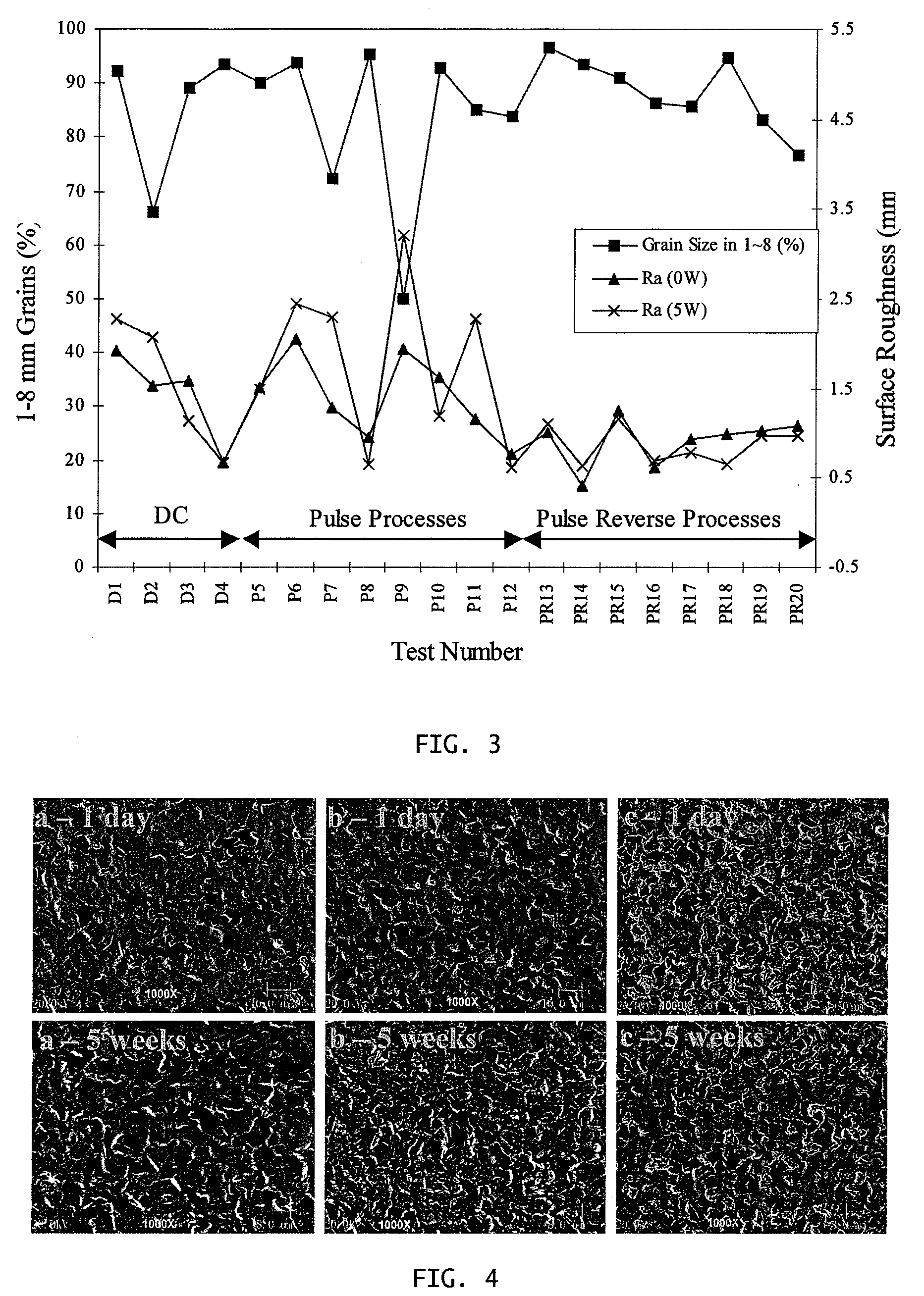
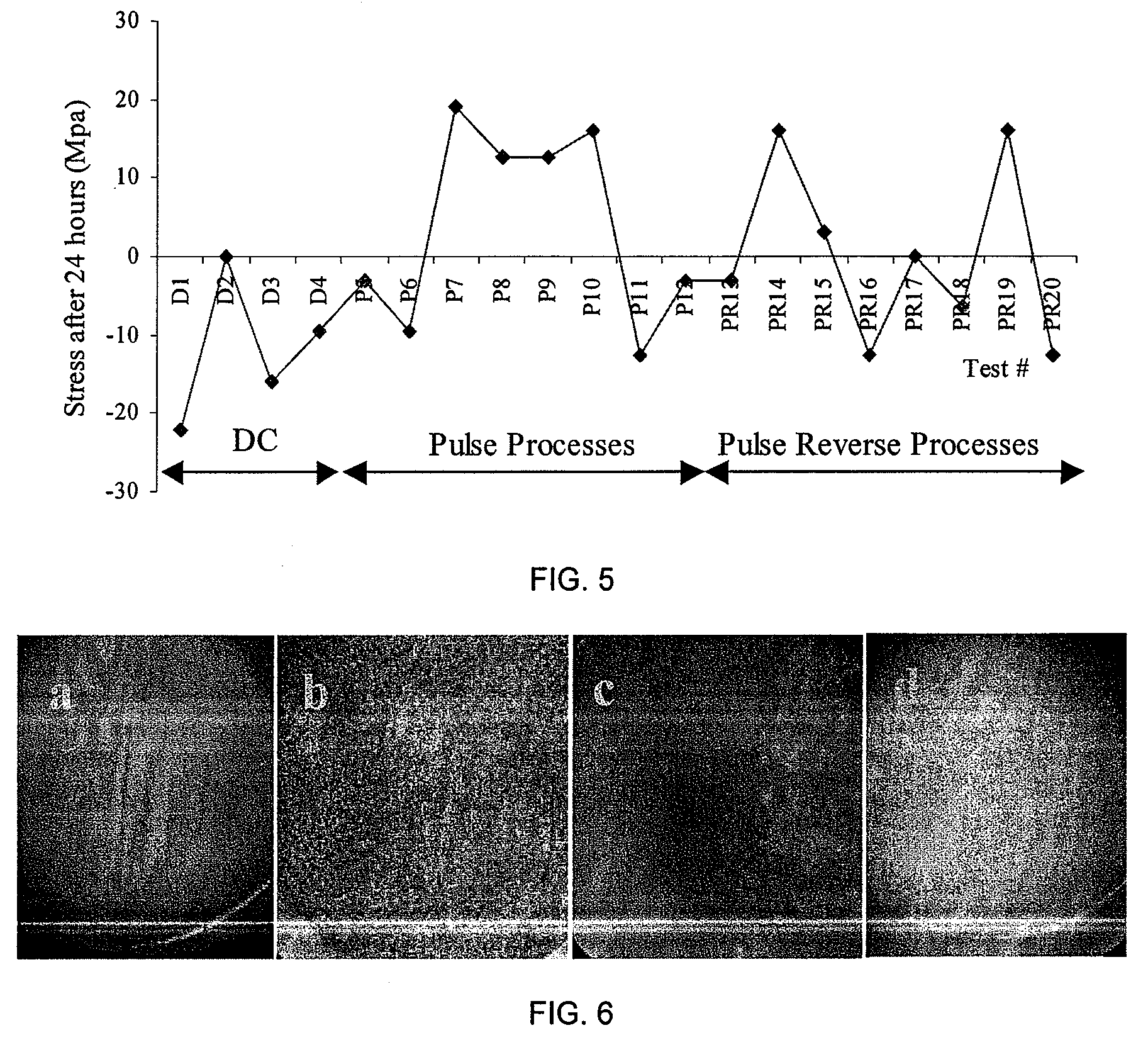
[0036]In the first test (D1), the rotation speed was 100 revolutions per minute and the average current density was 10 milliamperes per square centimeter. The following deposit properties were measured: 1) the surface appearance was a matte finish, 2) the process efficiency was 87 percent, 3) the average plating rate was 0.50 micrometers per minute, 4) the surface roughness 2 weeks after plating was 1.93 micrometers, 5) the surface roughness 6 weeks after plating was 2.28 micrometers, 6) the coverage of the tin deposit was not 100 percent of the total area, 7) the percentage of grains in the size range of 1 to 8 micrometers was 92.1 percent, 8) the full width half maximum (FWHM) of the x-ray diffraction curve data in the (420) plane was 0.090, 9) the full width half maximum (FWHM) of the x-ray diffraction curve data in the (411) plane was 0.091, 10) the internal stress was a compressive stress with a magnitude of 22 megapascals, and 11) after 2 and 6 weeks, no whisker growth ...

example 2

Test D2

[0037]In the second test (D2), the rotation speed was 400 revolutions per minute and the average current density was 10 milliamperes per square centimeter. The following deposit properties were measured: 1) the surface appearance was a matte finish, 2) the process efficiency was 96 percent, 3) the average plating rate was 0.68 micrometers per minute, 4) the surface roughness 2 weeks after plating was 1.54 micrometers, 5) the surface roughness 6 weeks after plating was 2.08 micrometers, 6) the coverage of the tin deposit was not 100 percent of the total area, 7) the percentage of grains in the size range of 1 to 8 micrometers was 66.2 percent, 8) the full width half maximum (FWHM) of the x-ray diffraction curve data in the (420) plane was 0.088, 9) the full width half maximum (FWHM) of the x-ray diffraction curve data in the (411) plane was 0.096, 10) there was no internal stress (zero stress), and 11) after 2 and 6 weeks, no whisker growth was observed.

example 3

Test D3

[0038]In the third test (D3), the rotation speed was 400 revolutions per minute and the average current density was 20 milliamperes per square centimeter. The following deposit properties were measured: 1) the surface appearance was a matte finish, 2) the process efficiency was 90 percent, 3) the average plating rate was 0.95 micrometers per minute, 4) the surface roughness 2 weeks after plating was 1.58 micrometers, 5) the surface roughness 6 weeks after plating was 1.14 micrometers, 6) the coverage of the tin deposit was not 100 percent of the total area, 7) the percentage of grains in the size range of 1 to 8 micrometers was 89.1 percent, 8) the full width half maximum (FWHM) of the x-ray diffraction curve data in the (420) plane was 0.084, 9) the full width half maximum (FWHM) of the x-ray diffraction curve data in the (411) plane was 0.083, 10) the internal stress was a compressive stress with a magnitude of 15.9 megapascals, and 11) after 2 and 6 weeks, no whisker growt...


PUM

PropertyMeasurementUnit
Fractionaaaaaaaaaa
Lengthaaaaaaaaaa
Timeaaaaaaaaaa

Abstract

A method for electrochemically plating tin or tin alloy onto a workpiece to provide a tin or tin alloy deposit on said workpiece having a stress differential and workpieces characterized by a tin or tin alloy deposit having a stress differential.

Description

CROSS REFERENCE TO RELATED APPLICATIONS[0001]The present application claims priority of U.S. Provisional Application No. 60 / 756,634 filed Jan. 6, 2006.FIELD OF THE INVENTION[0002]The present invention relates to a method and apparatus for deposition of tin or tin alloy on a workpiece such as a semiconductor wafer, wafer level package, chip scale package or printed circuit board.BACKGROUND OF THE INVENTION[0003]A tin or tin alloy plating process for surface finish or solder applications that does not contain lead is desired by the electronics industry due to environmental considerations. However, lead-free tin or tin alloy solders deposited using electrochemical techniques have shown a tendency to grow whiskers. These whiskers can cause short-circuiting, resulting in poor reliability and failure of the electronics component. A number of theories have been postulated as to the cause of the whisker growth and detrimental solder performance. The three main causes proposed are internal s...

Claims


Application Information

Patent Timeline
IPC IPC(8): C25D3/56C25D3/30
CPCC25D3/30C25D3/32H05K2203/1492C25D5/18H05K3/3473C25D3/60C25D5/627C25D5/617C25D5/611
Inventor TAYLOR, E. JENNINGSSUN, JENNY J.
Owner FARADAY TECH INC
Why Eureka
Try Eureka