Close loop electrophoretic deposition of semiconductor devices

a technology of electrophoretic deposition and semiconductor devices, applied in the direction of electrolysis components, electrophoretic coatings, coatings, etc., can solve the problems of difficult control of the geometry and thickness of the phosphor layer, inability to generate white light from the active layer, and non-uniform color temperatur

Active Publication Date: 2007-07-12
CREELED INC
View PDF8 Cites 500 Cited by
  • Summary
  • Abstract
  • Description
  • Claims
  • Application Information

AI Technical Summary

Benefits of technology

[0013] Basically, and in general terms, the present invention directed to improved systems and methods for electrophoretic deposition (EPD) of materials on semiconductor devices. One embodiment of a system according to the present invention for depositing a material on a semiconductor device, comprises a chamber holdi

Problems solved by technology

One disadvantage of conventional LEDs used for lighting applications is that they cannot generate white light from their active layers.
One disadvantage of this method is that it is often difficult to control the phosphor layer's geometry and thickness.
As a result, light emitting from the LED at different angles can pass through different amounts of conversion material, which can result in an LED with non-uniform color temperature as a function of viewing angle.
Using the syringe method the geometry and thickness of the epoxy containing the conversion material is har

Method used


Image

  • Close loop electrophoretic deposition of semiconductor devices
  • Close loop electrophoretic deposition of semiconductor devices
  • Close loop electrophoretic deposition of semiconductor devices

Examples


Embodiment Construction

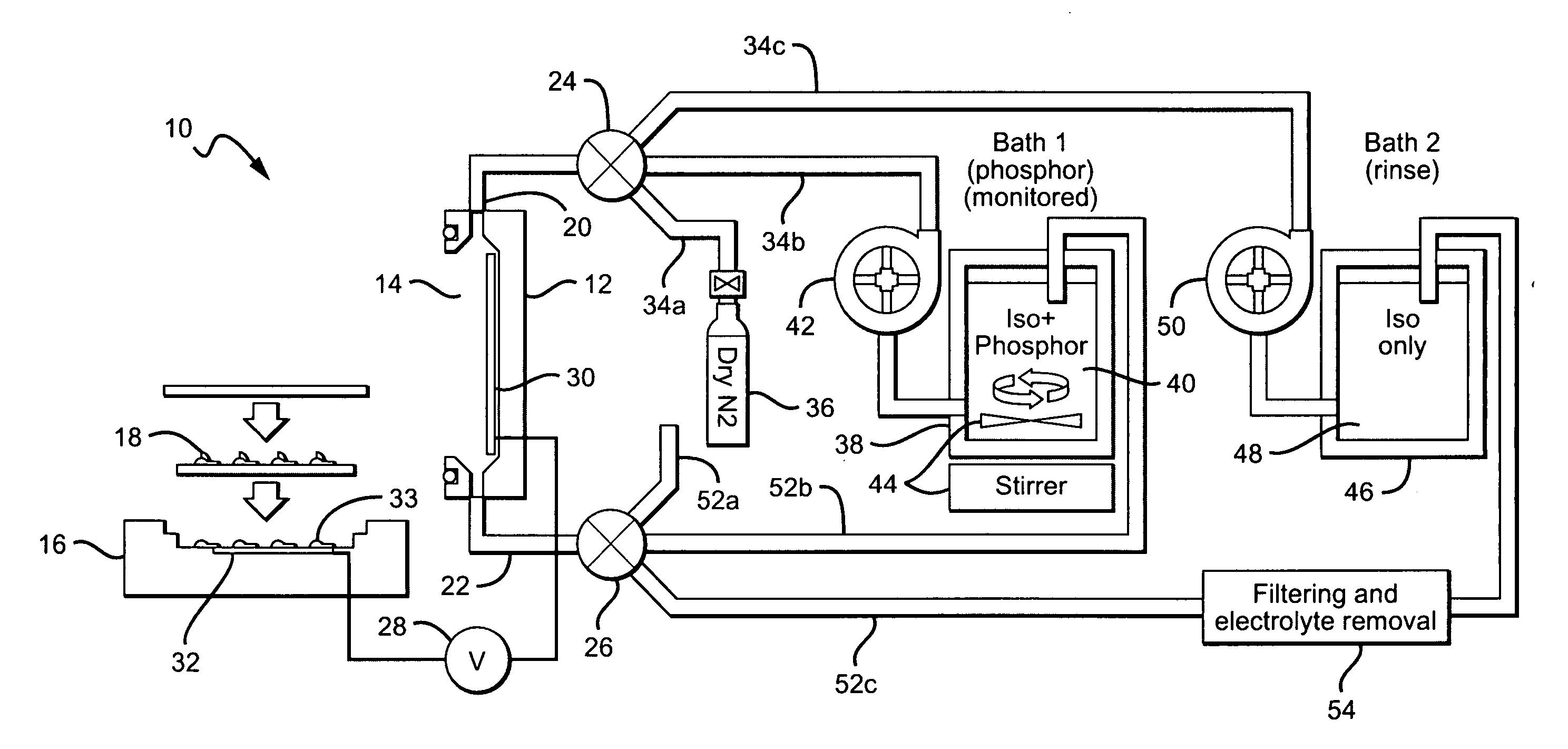
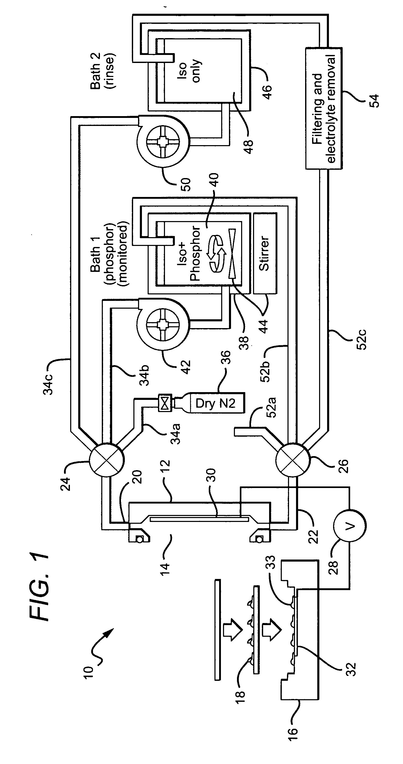
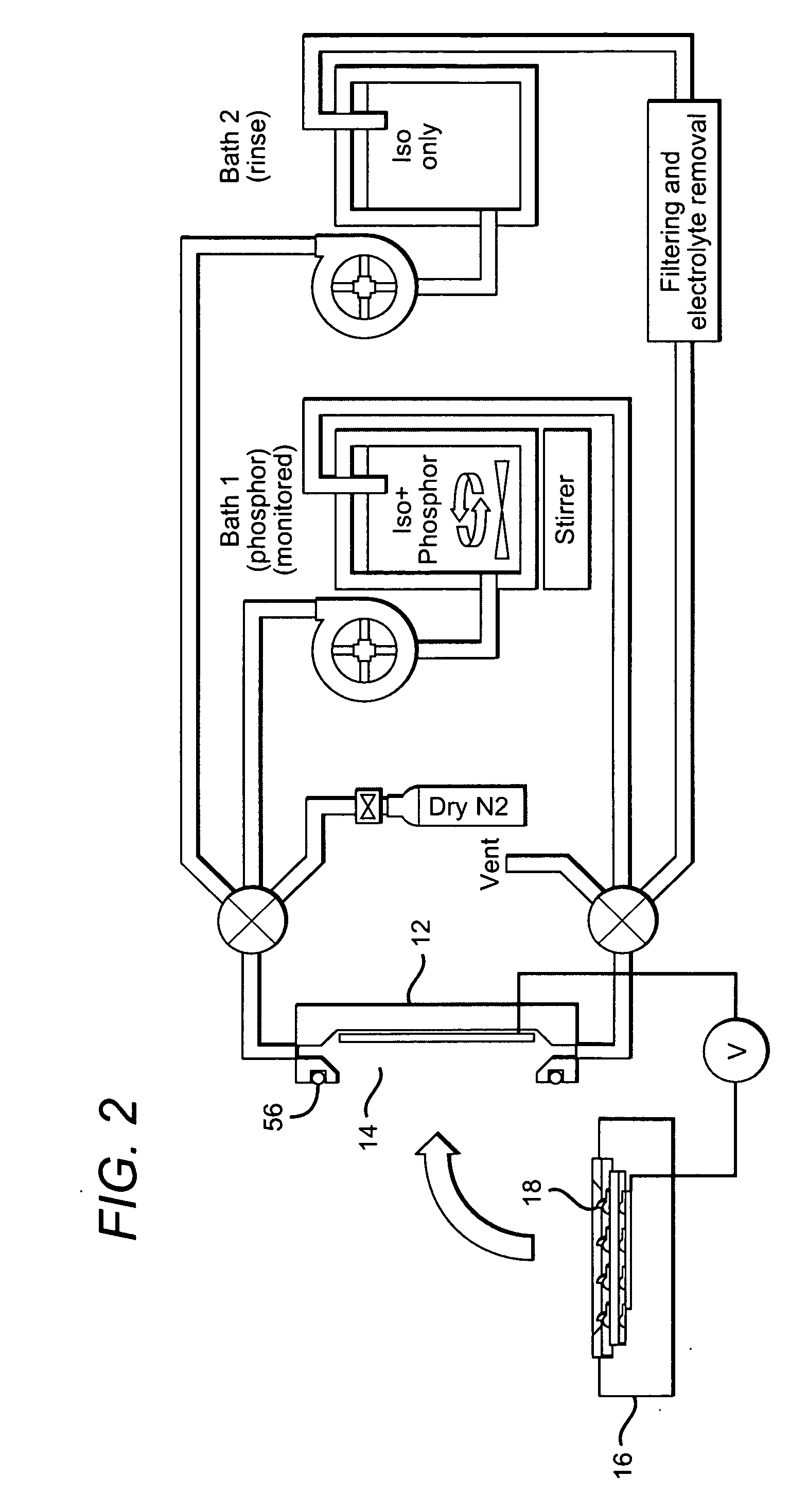
[0048] The present invention is generally directed to close loop systems and methods for electrophoretic deposition (EPD) of material on semiconductor devices. For purposes of this invention, close loop means that the solution containing the deposition material is not exposed to the ambient prior to or during the EPD process. In some embodiments, the solution is also not exposed to the surrounding ambient after the deposition process so that the solution can be used in subsequent EPD processes.

[0049] Close loop systems according to the present invention can deposit materials in solutions that are not contaminated by impurities and contaminants. Particularly, the solutions are free of water or moisture in the form of humidity that in the ambient air can be absorbed by the deposition solution. By being free of impurities and water, a uniform layer of the materials can be deposited on the semiconductor devices with the thickness of the layer being repeatable in subsequent EPD processe...


PUM

PropertyMeasurementUnit
Electric potential / voltageaaaaaaaaaa
Areaaaaaaaaaaa
Exposure limitaaaaaaaaaa

Abstract

One close loop system and method for electrophoretic deposition (EPD) of phosphor material on light emitting diodes (LEDs). The system comprises a deposition chamber sealed from ambient air. A mixture of phosphor material and solution is provided to the chamber with the mixture also being sealed from ambient air. A carrier holds a batch of LEDs in the chamber with the mixture contacting the areas of the LEDs for phosphor deposition. A voltage supply applies a voltage to the LEDs and the mixture to cause the phosphor material to deposit on the LEDs at the mixture contacting areas.

Description

[0001] This application claims the benefit of U.S. provisional application Ser. No. 60 / 711,590 to Tarsa et al., which was filed on Aug. 25, 2005.[0002] This invention was made with Government support under NIST (ATP) Contract No. 70NANB4H3037. The Government has certain rights in this inventionBACKGROUND OF THE INVENTION [0003] 1. Field of the Invention [0004] This invention relates to electrophoretic deposition of semiconductor devices and more particularly to electrophoretic deposition of light emitting diodes (LEDs) with a phosphor using a close loop system. [0005] 2. Description of the Related Art [0006] LEDs are solid-state devices that convert electric energy to light and they generally comprise an active layer of semiconductor material sandwiched between two oppositely doped layers. When a bias is applied across the doped layers, holes and electrons are injected into the active layer where they recombine to generate light that is emitted omnidirectionally from the active laye...

Claims


Application Information

Patent Timeline
IPC IPC(8): H01L33/00H01L33/50
CPCC25D13/12C25D13/22C25D15/00C25D21/00C25D5/003C25D7/123C25D13/02C25D17/02H01L2933/0041
Inventor TARSA, ERIC J.LEUNG, MICHAELKELLER, BERNDUNDERWOOD, ROBERTYOUMANS, MARK
Owner CREELED INC
Why Eureka
Try Eureka