Etching method of single wafer

a single-walled, etching technology, applied in the direction of decorative surface effects, electrical appliances, decorative arts, etc., can solve the problems of reducing the mechanical strength of the wafer, adversely affecting the electrical characteristics, and etching the disadvantageous side end portion of the wafer rear surfa

Inactive Publication Date: 2007-07-12
SUMCO CORP
View PDF1 Cites 14 Cited by
  • Summary
  • Abstract
  • Description
  • Claims
  • Application Information

AI Technical Summary

Benefits of technology

[0009] It is an object of the present invention to provide an etching method of a single wafer which can prevent an etchant from flowing to a wafer rear surface and uniformly etch not only a wafer front surface but also a wafer end portion while suppressing local shape collapse of the wafer end portion to the minimum level.
[0012] In the invention according to claim 1, an etching width taken by the etchant supplied for one process is reduced by intermittently supplying the etchant. After the etchant for one process is supplied, supply of the etchant is stopped, and the etchant for the next process is supplied after the supplied etchant flows off from the end portion of the wafer. Therefore, local shape collapse due to the etchant staying at the wafer end portion can be suppressed to the minimum level, and not only the wafer front surface but also the wafer end portion can be uniformly etched while preventing the etchant from flowing to the wafer rear surface. Moreover, since the etchant is intermittently supplied in the predetermined number of times, a desired etching width can be assured.
[0017] According to the etching method of a single wafer of the present invention, the etchant is intermittently supplied onto the front surface of the wafer in twice or more, supply of the etchant is stopped after the etchant for one process is supplied, and the etchant for the next process is supplied after the supplied etchant flows off from the end portion of the wafer. As a result, local shape collapse of the wafer end portion is suppressed to the minimum level, and not only the wafer front surface but also the wafer end portion can be uniformly etched while preventing the etchant from flowing to the wafer rear surface.

Problems solved by technology

The work-affected layer induces a crystal defect such as slip dislocation in a device manufacturing process, reduces a mechanical strength of the wafer and adversely affects electrical characteristics, and hence this layer must be completely removed.
However, a part of the etchant flows to a wafer rear surface side end portion and a wafer rear surface from the wafer front surface side end portion so that the wafer rear surface side end portion and the wafer rear surface are disadvantageously etched.
Therefore, when the processing liquid is an etchant, there is a problem that a position where the etchant stays is etched beyond necessity and a shape of the wafer end portion subjected to a chamfering process locally collapses.

Method used


Image

  • Etching method of single wafer
  • Etching method of single wafer
  • Etching method of single wafer

Examples


example 1

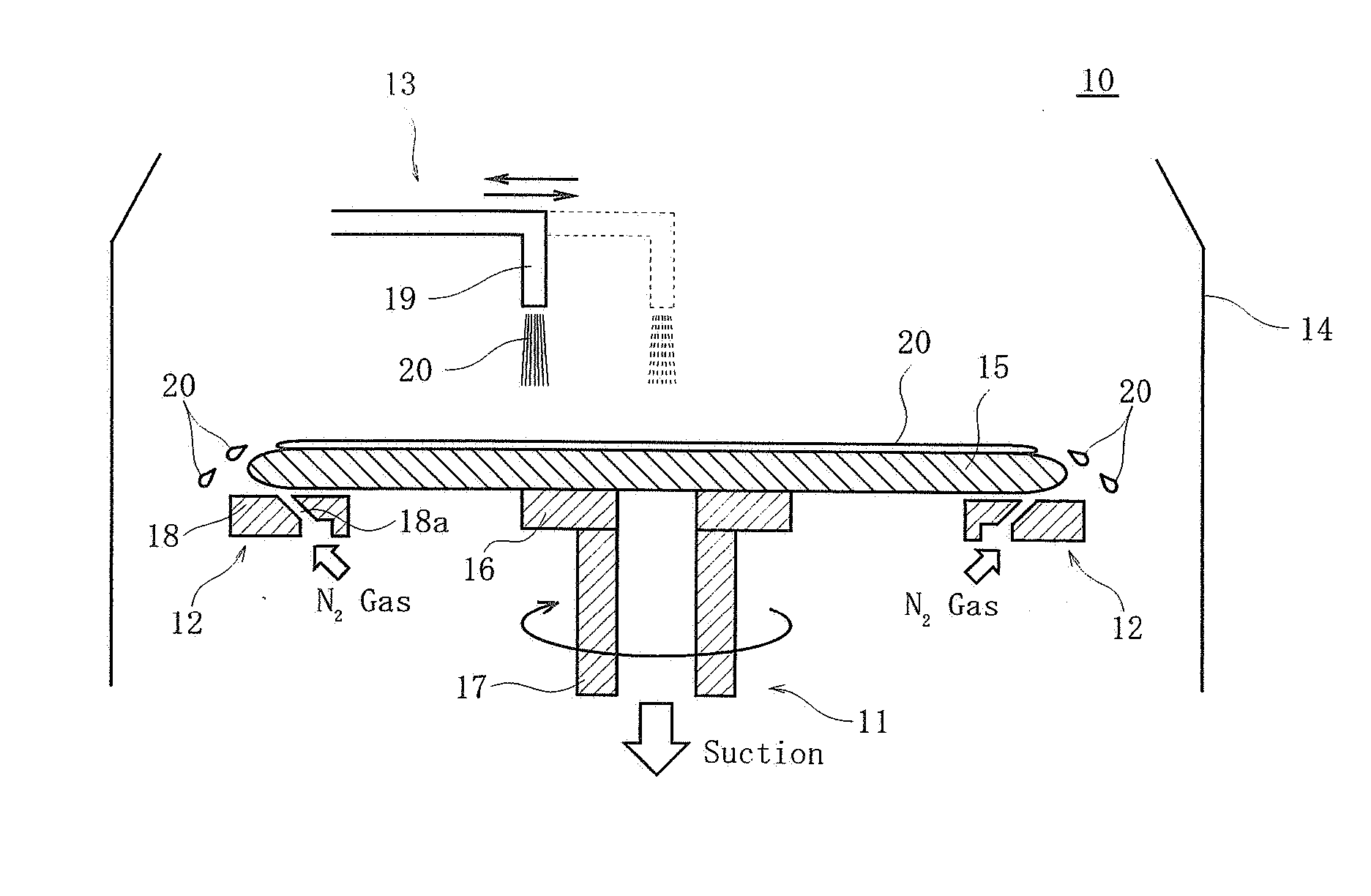
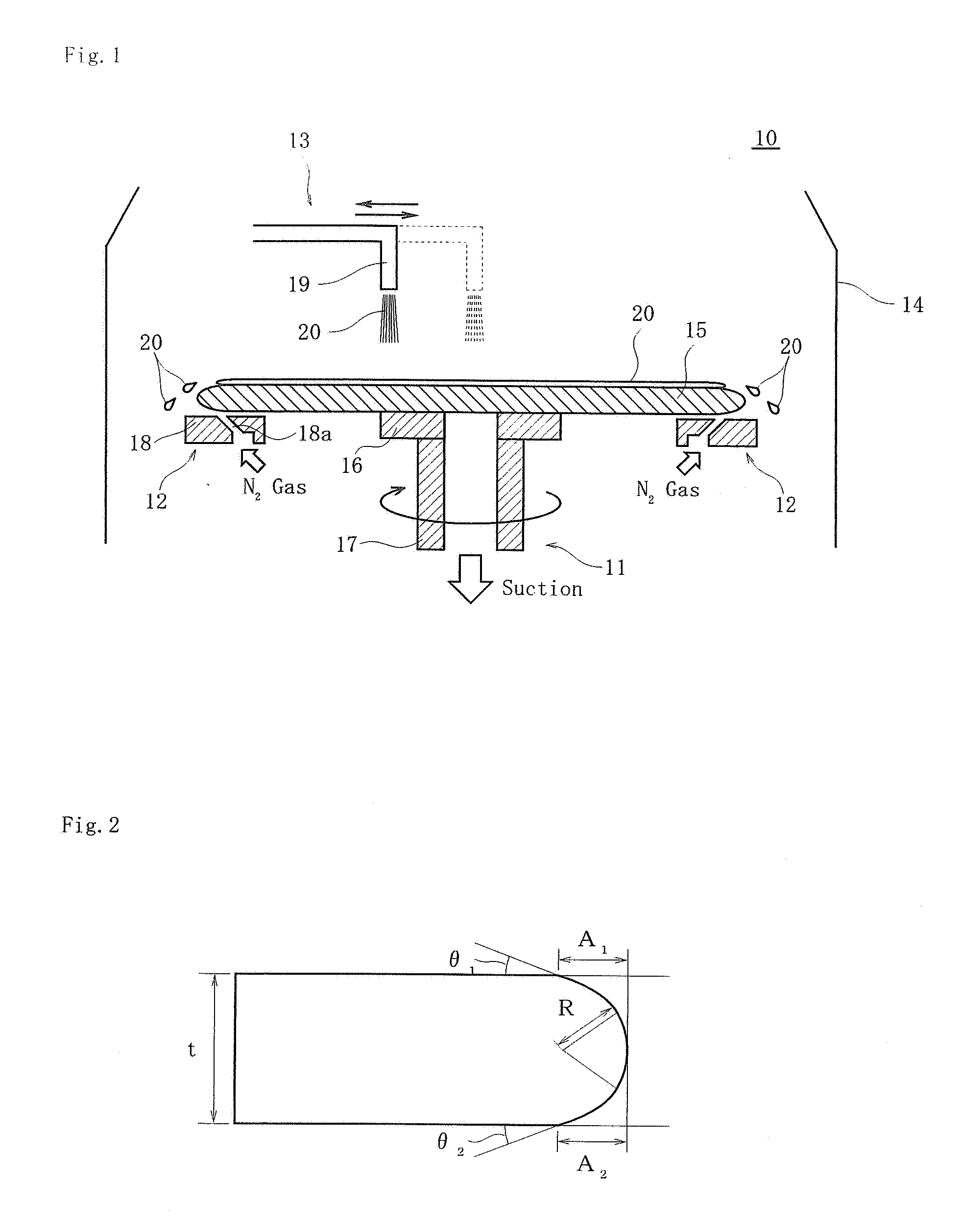
[0037] First, there was prepared a silicon wafer of 300 mmφ having a chamfered end portion and flattened front and rear surfaces. Further, there was also prepared an etchant containing HF, HNO3, H3PO4 and H2O at a mixture weight ratio of 7.0%:31.7%:34.6%:26.7%. FIG. 2 shows a cross-sectional shape of the chamfered wafer. In FIG. 2, reference character t denotes a thickness of the wafer; A1, a chamfer width on a wafer front surface side; A2, a chamfer width on a wafer rear surface side; R, a curvature radius of a wafer end portion; θ1, a chamfer angle of a wafer front surface side end portion; and θ2, a chamfer angle of a wafer rear surface side end portion.

[0038] Then, the wafer was mounted on a chuck of a single wafer etching apparatus shown in FIG. 1 in such a manner that the front surface becomes an upper surface. Subsequently, the wafer was horizontally rotated, the etchant was supplied onto the upper surface of the wafer from a supply nozzle provided above the wafer, and the e...


PUM

PropertyMeasurementUnit
widthaaaaaaaaaa
widthaaaaaaaaaa
degree of flatnessaaaaaaaaaa

Abstract

Local shape collapse of a wafer end portion is suppressed to the minimum level, and a wafer front surface as well as a wafer end portion is uniformly etched while preventing an etchant from flowing to a wafer rear surface. There is provided an etching method of a single wafer which supplies an etchant onto a wafer front surface in a state where a single wafer having flattened front and rear surfaces is held, and etches the wafer front surface and a front surface side end portion by using a centrifugal force generated by horizontally rotating the wafer. According to this method, the etchant is intermittently supplied onto the front surface of the wafer in twice or more, supply of the etchant is stopped after the etchant for one process is supplied, and the etchant for the next process is supplied after the supplied etchant flows off from the end portion of the wafer.

Description

BACKGROUND OF THE INVENTION [0001] 1. Field of the Invention [0002] The present invention relates to an etching method of a single wafer which can uniformly etch not only a wafer front surface but also a wafer end portion while suppressing local shape collapse of the wafer end portion to the minimum level. [0003] 2. Description of the Related Art [0004] Generally, a semiconductor wafer manufacturing process is constituted of steps of subjecting a wafer obtained by cutting and slicing a single-crystal ingot to chamfering, machine polishing (lapping), etching, mirror grinding (polishing) and cleaning, and produces a wafer having a highly accurate degree of flatness. The wafer subjected to machining processes such as block cutting, external-diameter grinding, slicing, lapping and others has a damage layer, i.e., a work-affected layer on a surface thereof. The work-affected layer induces a crystal defect such as slip dislocation in a device manufacturing process, reduces a mechanical st...

Claims


Application Information

Patent Timeline
Patent Type & Authority Applications(United States)
IPC IPC(8): C03C15/00H01L21/302
CPCH01L21/02019H01L21/02087H01L21/6708H01L21/67075H01L21/30608H01L21/302H01L21/306
Inventor KOYATA, SAKAEHASHII, TOMOHIROMURAYAMA, KATSUHIKOTAKAISHI, KAZUSHIGEKATOH, TAKEO
Owner SUMCO CORP
Why Eureka
Try Eureka