
Active cancellation matrix for process parameter measurements

a technology of process parameter and active cancellation, applied in the field of integrated circuit design and testing, can solve the problems of large number of cells, difficult physical design without the aid of computers, and complicated connections between cells

Inactive Publication Date: 2007-07-19
IBM CORP
View PDF8 Cites 5 Cited by
  • Summary
  • Abstract
  • Description
  • Claims
  • Application Information

AI Technical Summary

Benefits of technology

The present invention provides an improved method for testing electronic devices in an integrated circuit. The method takes into consideration the loading effects of transmission wires in the testing circuitry and can easily be applied to a row and column structure of devices under test. The method involves using a matrix of source inputs, voltage rails, and feedback rails to generate and adjust voltage signals for testing the devices. The method can also include using a digital-to-analog converter and measuring current for varying input voltages to establish I-V curves for the devices. The technical effects of the invention include improved accuracy and efficiency in testing electronic devices in integrated circuits.

Problems solved by technology

An IC may include a very large number of cells and require complicated connections between the cells.
Due to the large number of components and the details required by the fabrication process for very large scale integrated (VLSI) devices, physical design is not practical without the aid of computers.
While the outputs of circuit 2 provide a fair basis to characterize the response of the devices, the measurements are not completely accurate since they fail to take into consideration loading effects on signal transmission.
Calibration of the measurement circuitry does not compensate for variations in the loading effects.
They all use discrete components, that is, separate circuit structures, which facilitates remote sensing, but there are problems with applying these techniques to testing of electronic devices.
Because of their discrete nature, it is difficult to implement these designs in a single integrated circuit.
Also, none of these techniques can be rasterized, i.e., applied to an array of columns and rows of devices.

Method used


Image

  • Active cancellation matrix for process parameter measurements
  • Active cancellation matrix for process parameter measurements
  • Active cancellation matrix for process parameter measurements

Examples


Embodiment Construction

)

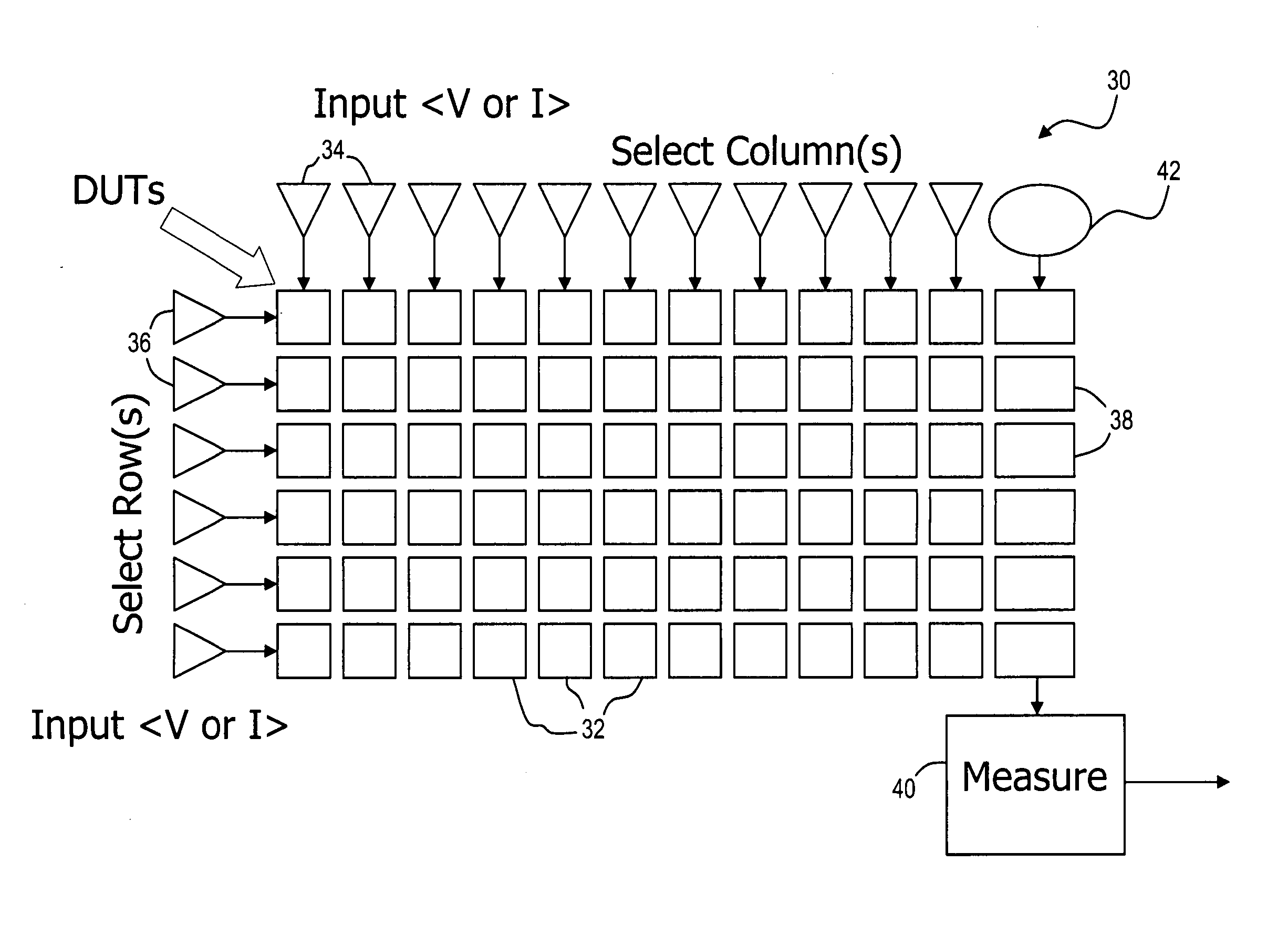
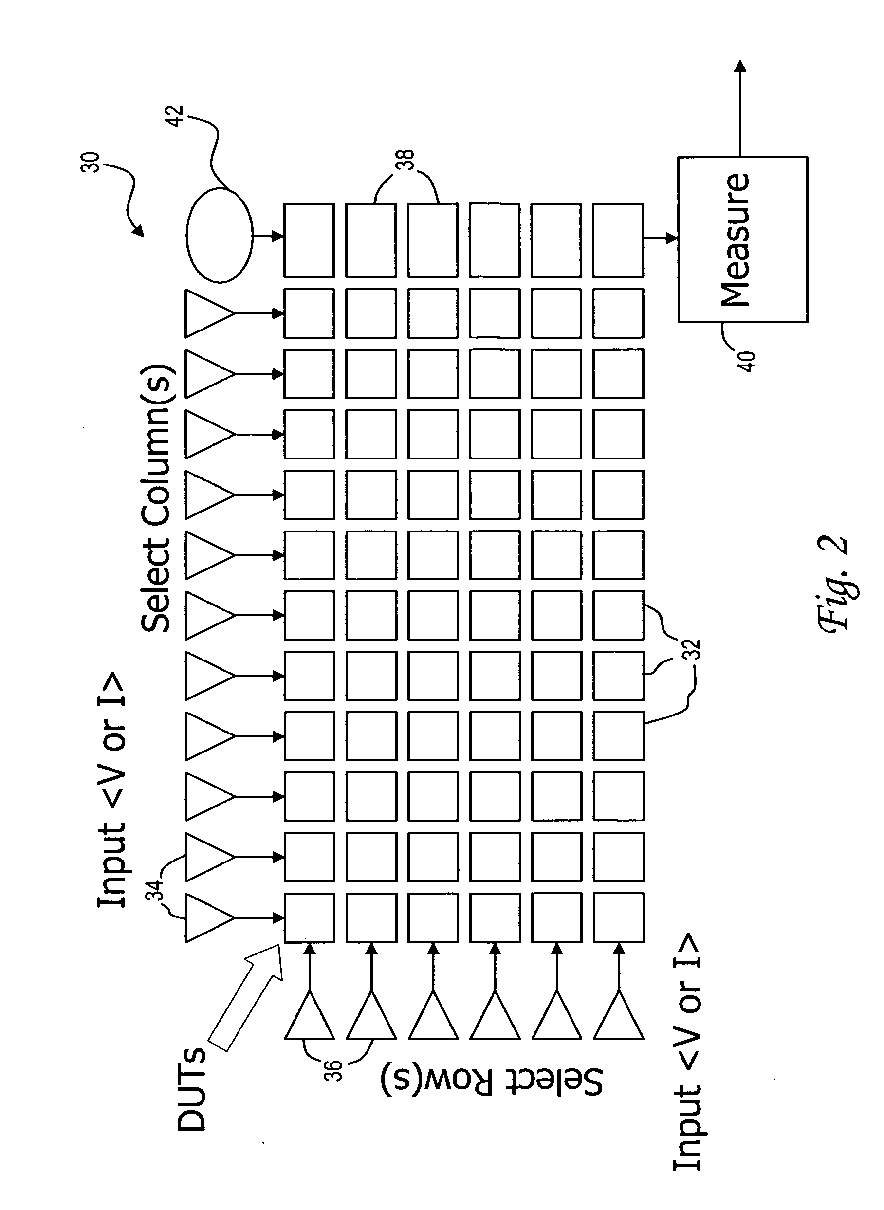
[0024] With reference now to the figures, and in particular with reference to FIG. 2, there is depicted one embodiment 30 of a test system constructed in accordance with the present invention. Test system 30 may be formed as part of a single integrated circuit (IC) test chip having various types of electronic devices to be tested, and is generally comprised of a plurality of devices under test (DUTs) 32, a plurality of column inputs 34, a plurality of row inputs 36, a plurality of selectors 38, a measurement unit 40, and selector control logic 42. DUTs 32 are arranged in a matrix or array having rows and columns. In this example there are six rows and eleven columns. DUTs 32 can be single elements such as a transistor, or more complicated circuit structures. DUTs 32 can also be as simple as sections of interconnects with vias and contacts.

[0025] The input signals may be any parameter of interest, such as voltage or current. For example, when the DUTs are transistors, test system 3...


PUM


Abstract

An active cancellation matrix for process parameter measurements provides feedback paths for each test location wherein each feedback path is used to sense the applied voltage and the sensed voltage is used to adjust the source voltage for any variations along the input path. The devices under test are arranged in a row and column array, and the feedback and voltage input paths are formed along respective rails which extend generally parallel to a row of devices under test. Selectors are used to selectively route the outputs of the test nodes to a measurement unit such as a current sensor. The input voltages can be varied to establish current-voltage (I-V) curves for the devices under various conditions. In the example where the devices under test are transistors, each source input includes three voltage inputs (rails) for a drain voltage, a source voltage, and a gate voltage.

Description

[0001] This invention was made with Government support under DARPA, NBCH3039004. THE GOVERNMENT HAS CERTAIN RIGHTS IN THIS INVENTION.BACKGROUND OF THE INVENTION [0002] 1Field of the Invention [0003] The present invention generally relates to the design and testing of integrated circuits, and more particularly to a method and system for testing an array of electronic devices. [0004] 2. Description of the Related Art [0005] Integrated circuits are used for a wide variety of electronic applications, from simple devices such as wristwatches, to the most complex computer systems. A microelectronic integrated circuit (IC) chip can generally be thought of as a collection of logic cells with electrical interconnections between the cells, formed on a semiconductor substrate (e.g., silicon). An IC may include a very large number of cells and require complicated connections between the cells. A cell is a group of one or more circuit elements such as transistors, capacitors, resistors, inductor...

Claims


Application Information

Patent Timeline
Patent Type & Authority Applications(United States)
IPC IPC(8): G01R31/26
CPCG01R31/3004G11C2029/5006G11C2029/5002G11C29/50
Inventor GEBARA, FADI H.LIU, YINGSIVAGNANAME, JAYAKUMARANVO, IVAN
Owner IBM CORP
Learn More