Imaging apparatus

a technology of smear correction and apparatus, applied in the field of smear correction technique, can solve the problems of reducing the accuracy of photometry and color measurement, blown highlights, and smear-shaped noises or darkened screens, and achieve the effects of reducing analog gain or iso sensitivity, reducing the influence of smear, and improving image quality

Inactive Publication Date: 2007-07-19
FUJIFILM CORP
View PDF7 Cites 49 Cited by
  • Summary
  • Abstract
  • Description
  • Claims
  • Application Information

AI Technical Summary

Benefits of technology

[0024]The imaging apparatus according to the ninth aspect enables suppression of influences of a smear and improvement of image quality by lowering analog gain or ISO sensitivity when the smear has occurred in a wide area across the entire screen or when the smear is intense.
[0025]According to the present invention, smear correction capabilities may be enhanced not only in the smear occurrence position, and exposure control (AE), white balance control, chroma suppress processing, gamma correction or the like may be performed in an appropriate manner even when during a occurrence of a smear.

Problems solved by technology

In conventional smear correction circuits, in the event that the proportion of a smear component (including a blooming component) to a total screen is significant, a problem may arise in that the subtrahend in relation to the signal at the horizontal pixel position of the smear becomes too large (overcompensation), causing stripe-shaped noises or darkened screens, or otherwise the smear is insufficiently compensated and results in blown highlights.
In addition, there is another problem in that such occurrences of stripe-shaped noises and blown highlights as described above reduces accuracy of photometry and color measurement, in turn reducing the accuracy of exposure control (AE) and white balance compensation (AWB).

Method used


Image

  • Imaging apparatus
  • Imaging apparatus
  • Imaging apparatus

Examples


first embodiment

[0062]The above-mentioned smear correction circuit 48 will now be described. FIG. 4 is a block diagram showing a smear correction circuit according to a first embodiment of the present invention.

[0063]A smear correction circuit 48-1 shown in FIG. 4 comprises an adder circuit 100, a line memory 102, a memory controller 104, an OB position detection counter 106, a divider circuit 108, a smear detection circuit 110, a smear correction value calculation circuit 112, a smear occurrence position storage circuit 116, and a subtraction circuit 114.

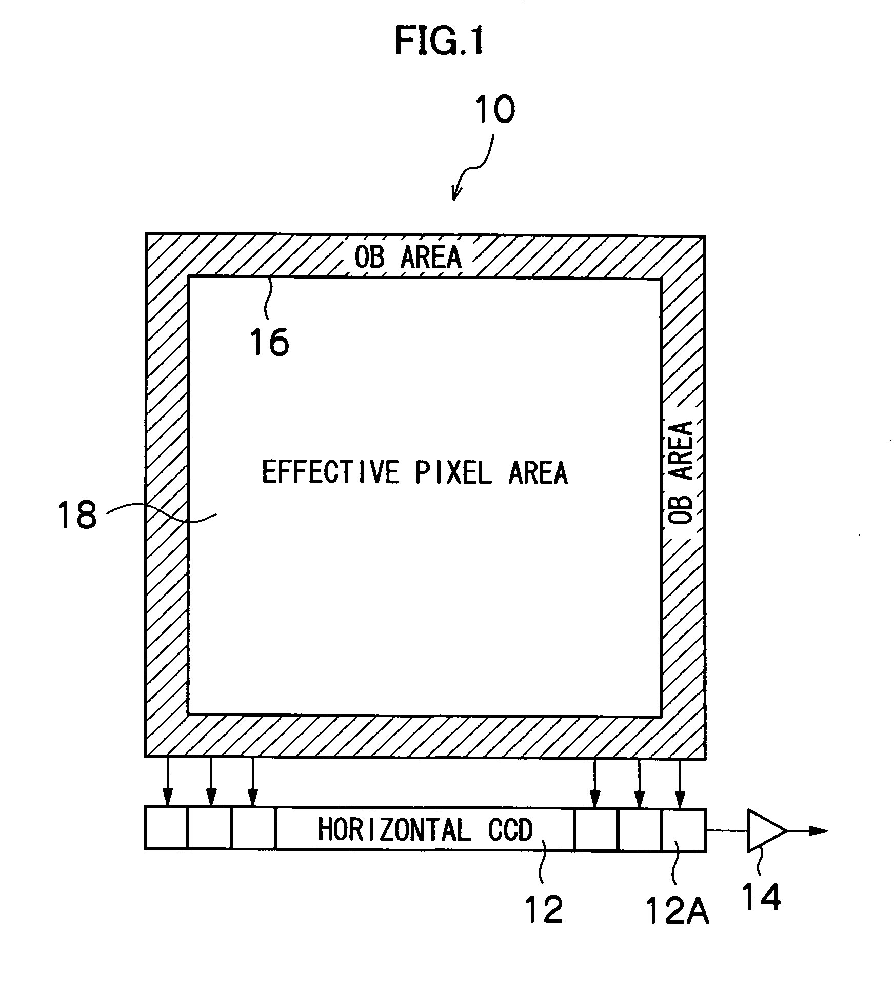
[0064]The adder circuit 100 is arranged so that 8-bit data among the 12-bit CCD-RAW data from the AFE 30 is inputted thereto. The 8 bits are, for example, low-order 8 bits of the 12 bits. However, the low-order 8 bits need not be the first to eighth low-order bits, and for instance, may instead be the third to tenth low-order bits. This is because the characteristics of the smear signal allow compression to be performed on an area which does not r...

second embodiment

[0079]A second embodiment of the present embodiment will now be described. FIG. 8 is a block diagram showing a smear correction circuit according to the second embodiment of the present invention. In the following description, the same components as in the first embodiment shown in FIG. 4 are designated by the same reference numerals, and detailed description thereof will be omitted.

[0080]A smear correction circuit 48-2 shown in FIG. 8 comprises an adder circuit 100, a line memory 102, a memory controller 104, an OB position detection counter 106, a divider circuit 108, a smear detection circuit 110, a smear correction value calculation circuit 112, a smear occurrence position storage circuit 116, a subtraction circuit 114, and a smear occurrence proportion calculation / storage circuit 118.

[0081]The smear occurrence proportion calculation / storage circuit 118 is a device which calculates and stores a proportion of the smear occurrence area to the entire effective pixel area (smear occ...

third embodiment

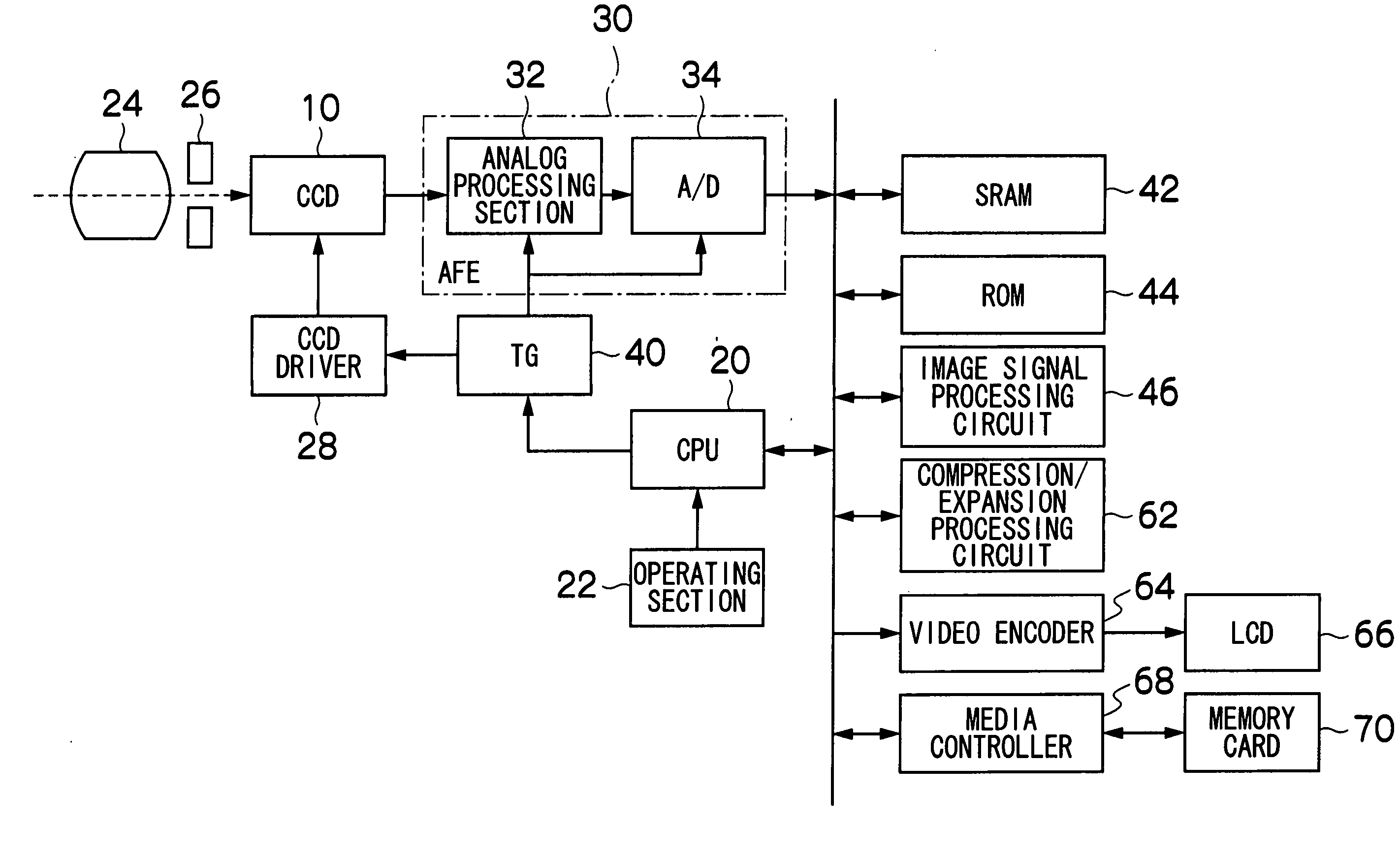
[0087]A third embodiment of the present embodiment will now be described. FIG. 10 is a block diagram showing an image signal processing circuit according to the third embodiment of the present invention. As shown in FIG. 10, an image signal processing circuit 46 comprises a smear correction circuit 48, a black level correction circuit 50, a white balance adjustment circuit 52, a gamma correction circuit 54, a YC conversion circuit 56, a contour correction circuit 58 and a color-difference matrix circuit 60, and further comprises a photometric area specification section 72.

[0088]FIG. 11 is a flowchart for illustrating a flow of processing of a smear correction method according to the third embodiment of the present invention. First, when data (CCD-RAW data) is inputted from the AFE 30, determination is made on whether the data is related to an OB area (step S50). If it is determined that the data relates to an OB area, an average value of all the data of the OB area (average OB value...


PUM


Abstract

An aspect of the present invention provides an imaging apparatus comprising: a solid-state image sensor having an effective pixel area and an optical black area; a smear detection device which detects smear intensity and smear occurrence position in a smear occurrence area, in which a smear occurs, in the effective pixel area, based on an output signal obtained from the optical black area of the solid-state image sensor; and a smear correction device which performs smear correction by subtracting a smear correction value corresponding to the smear intensity from an output signal of the smear occurrence area and the vicinity thereof in the effective pixel area.

Description

BACKGROUND OF THE INVENTION[0001]1. Field of the Invention[0002]The present invention relates to an imaging apparatus, and in particular, to a smear correction technique for an imaging apparatus, such as a digital camera and a video camera, having a function for preventing degradation of image quality due to a smear phenomenon.[0003]2. Description of the Related Art[0004]When an image of a high-luminance object, such as the sun or a light, is photographed using an imaging apparatus having a charge coupled device (CCD) image sensor, a bright line in the form of a vertically extending stripe appears in the photographed image. Such a phenomenon is called a smear phenomenon, which is caused by leakage of a charge of a significant portion of incident light during transfer to a vertical transfer channel and subsequent read-out of charges created on the photodiodes (photoelectric conversion elements) of the CCD to the vertical transfer channel, or by leakage of the incident light itself to...

Claims


Application Information

Patent Timeline
Patent Type & Authority Applications(United States)
IPC IPC(8): H04N9/64H04N5/238H04N5/335H04N5/359H04N5/369H04N5/372H04N5/3728H04N9/04H04N9/07
CPCH04N5/2351H04N5/3595H04N5/361H04N9/735H04N9/045H04N9/646H04N5/3655H04N23/71H04N25/625H04N25/673H04N25/63H04N23/84H04N23/88
Inventor TAKANE, YASUO
Owner FUJIFILM CORP
Why Eureka
Try Eureka