

MOS transistor with elevated source and drain structures and method of fabrication thereof
a technology of source and drain structure and mos transistor, which is applied in the direction of transistors, electrical devices, semiconductor devices, etc., can solve the problems of short channel effect, impact on switching performance, and general phenomenon of scaled-down mos transistor, and achieve the effect of increasing the effective channel length and limiting the diffusion of dopan
- Summary
- Abstract
- Description
- Claims
- Application Information
AI Technical Summary
Benefits of technology
Problems solved by technology
Method used
Image

Examples
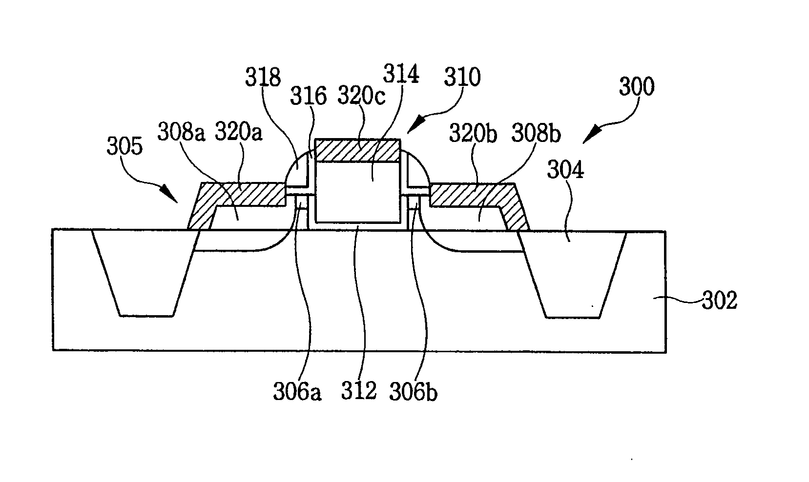
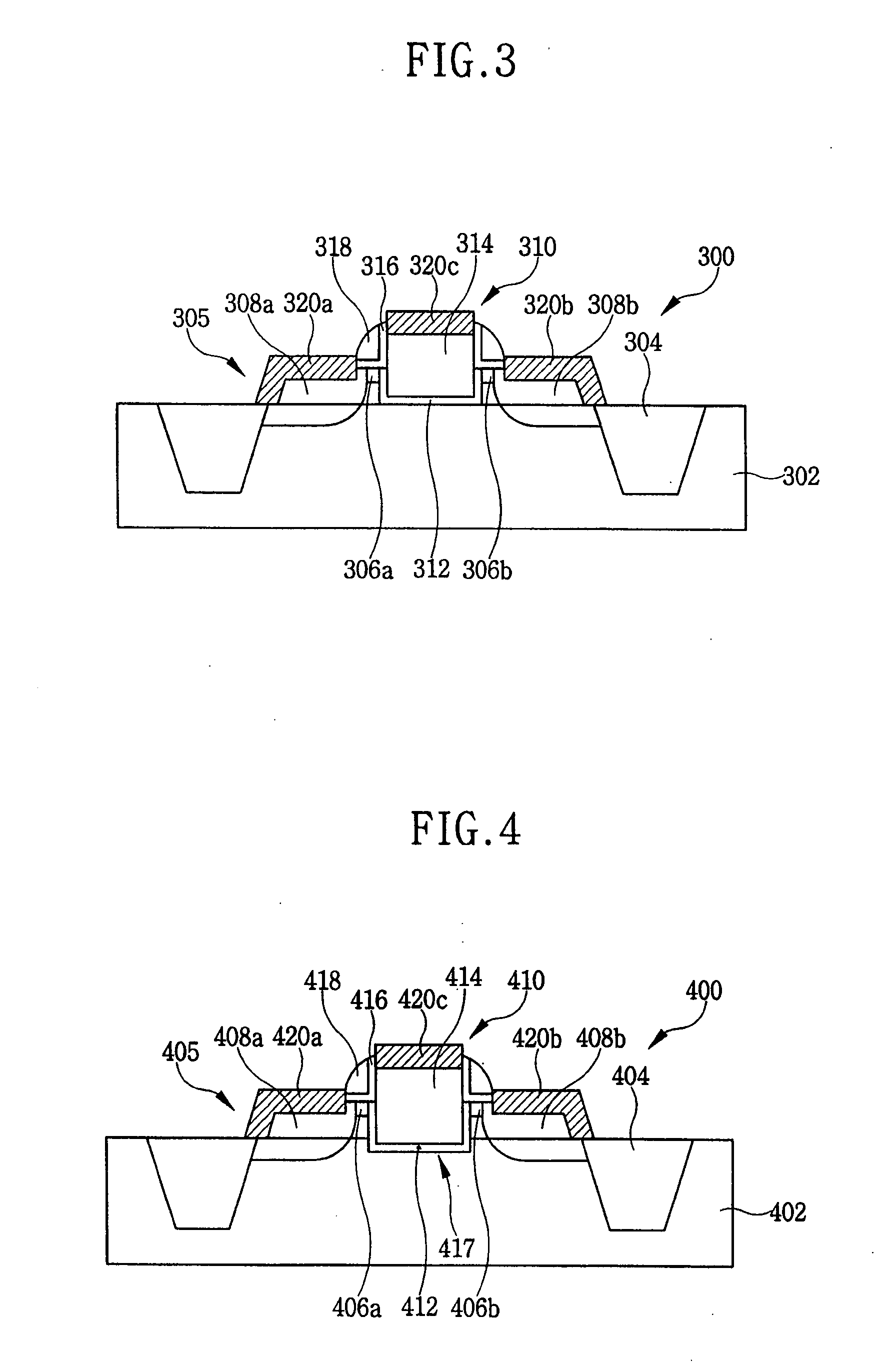
second embodiment
[0063] A second embodiment of the invention is shown and described above with reference to FIG. 4. In the second embodiment, the gate electrode 414 is formed in a trench or a recessed portion 417 of the semiconductor substrate 402. Other components of the transistor configuration of the second embodiment are similar to those of the first configuration above, and therefore their description will be omitted here. Components of FIG. 4 having a reference numeral beginning with the prefix “4” and a unique suffix “4xx” share the same purpose as those components of FIG. 3, described above, having the same suffix “3xx”.
[0064] A method of fabricating a semiconductor device according to the second embodiment of the present invention will now be described with reference to FIGS. 10A-10C.
[0065] The processes preceding the step shown at FIG. 10A are identical to those shown in FIGS. 9A-9D above with reference to the first embodiment.
[0066] Referring to FIG. 10A, the dummy gate, including the ...
PUM
 Abstract
Description
Claims
Application Information