

Pre-anneal of cosi, to prevent formation of amorphous layer between ti-o-n and cosi
- Summary
- Abstract
- Description
- Claims
- Application Information
AI Technical Summary
Benefits of technology
Problems solved by technology
Method used
Image

Examples
Embodiment Construction
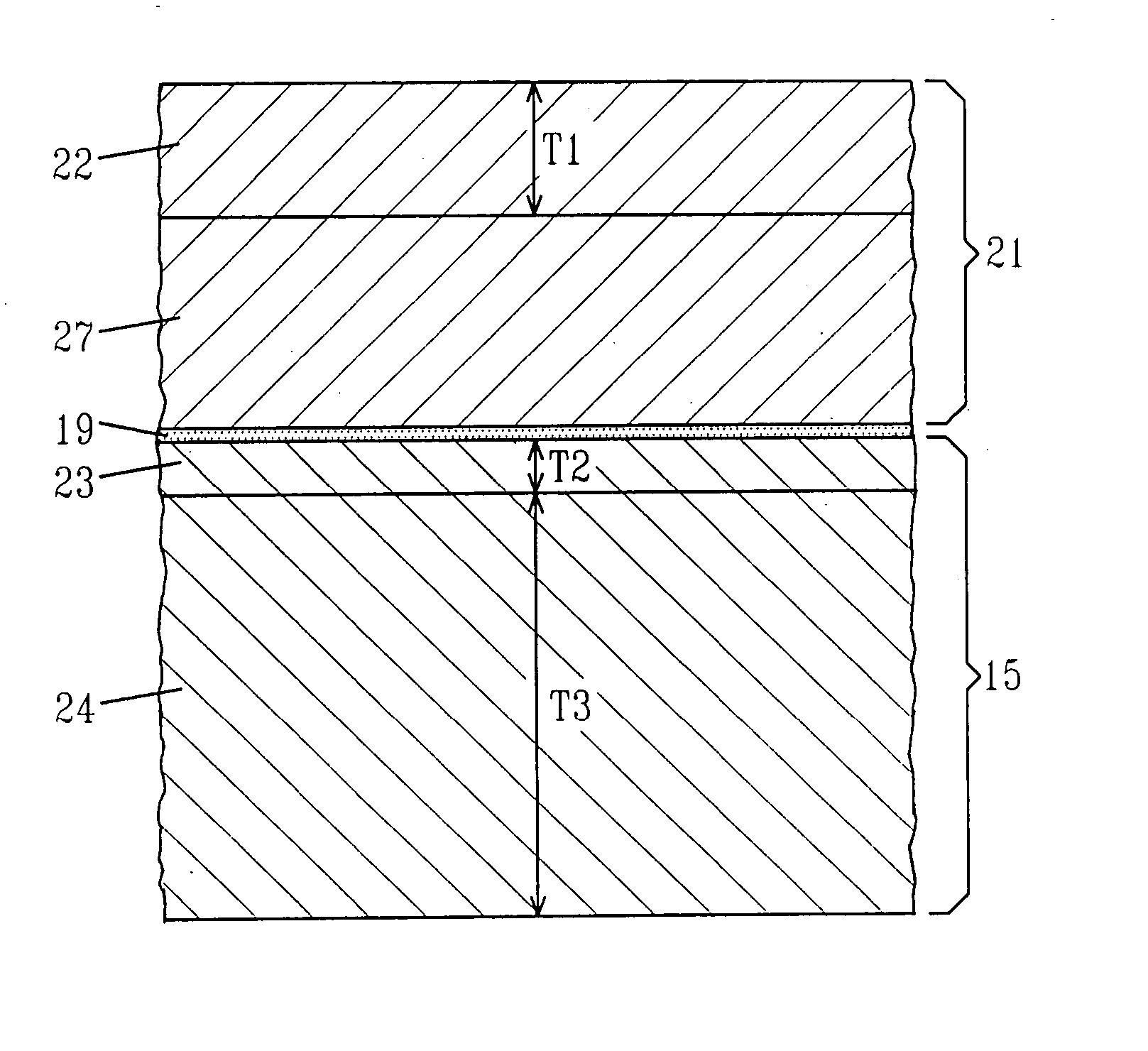
[0033] The inventive method for forming a low resistance via will now be discussed in greater detail referring to the drawings accompanying the present invention. It is noted in the accompanying drawings like and corresponding elements are referred to by like reference numbers.
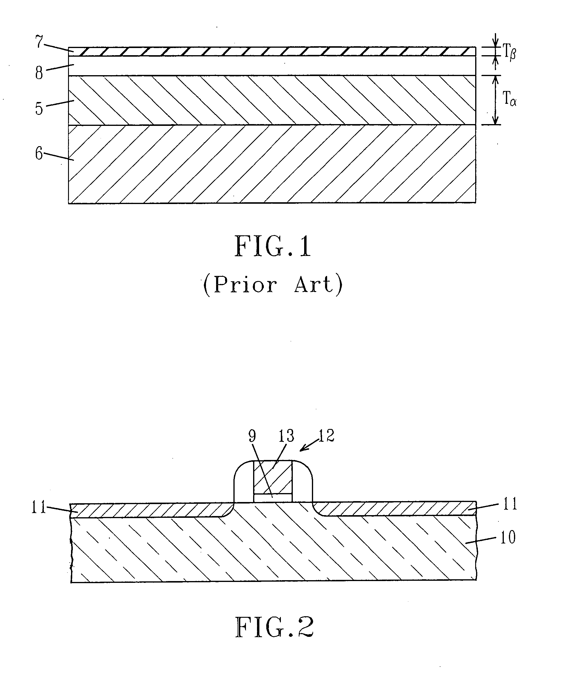
[0034] Referring to FIG. 2, a substrate 10 of silicon-containing material is first provided. Silicon-containing materials include, but are not limited to: silicon, single crystal silicon, polycrystalline silicon, silicon germanium, silicon-on-silicon germanium, amorphous silicon, silicon-on-insulator (SOI), silicon germanium-on-insulator (SGOI), and annealed polysilicon. The substrate may further comprise the source / drain regions 11 and gate region 12 of a complementary metal oxide semiconducting device. The gate region 12 may include a gate dielectric 9 and polysilicon gate conductor 13.
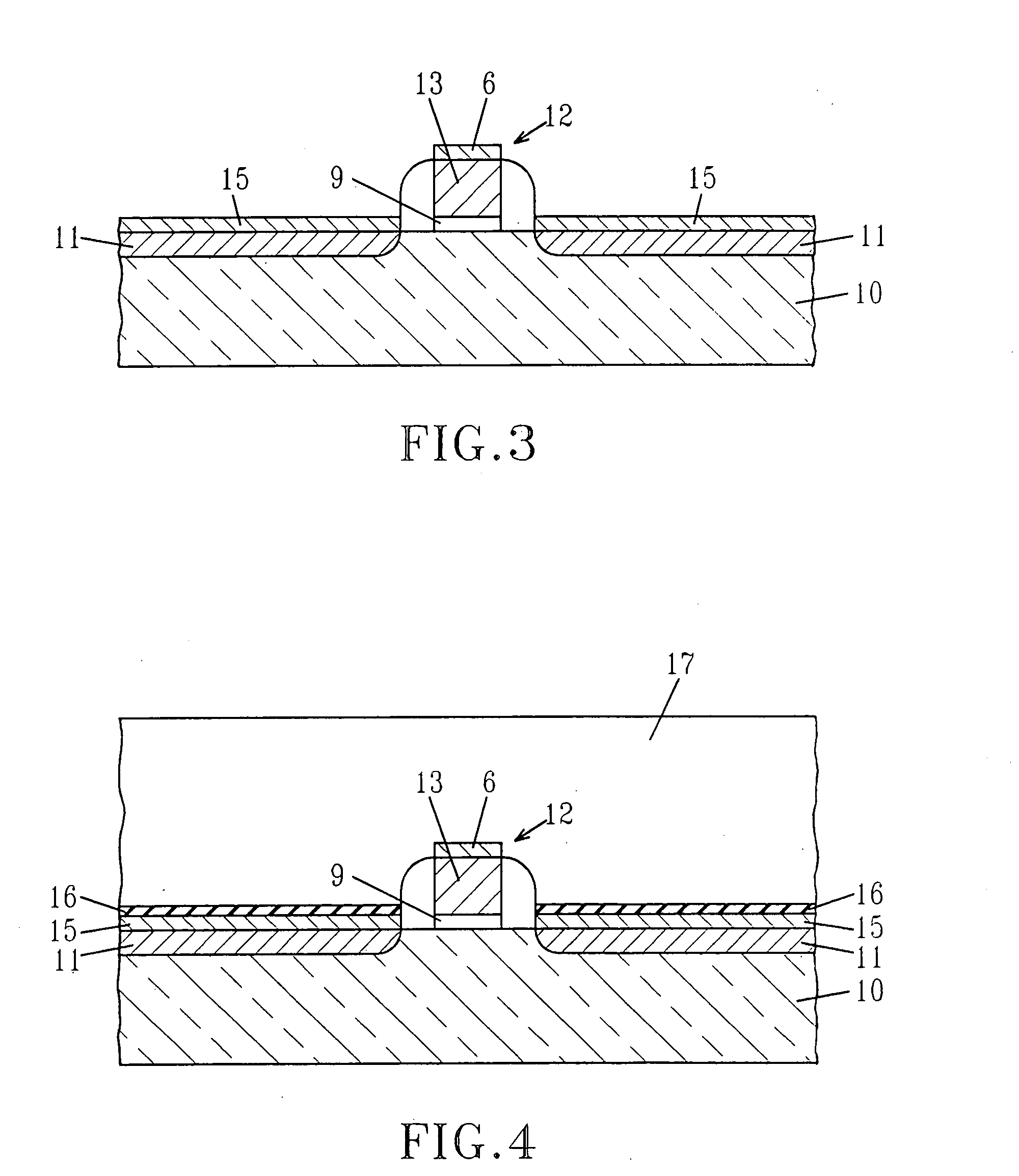
[0035] Referring to FIG. 3, a silicide region 15 is then formed atop the source and drain regions 11. A gate silicide regi...
PUM
 Abstract
Description
Claims
Application Information