Supercharge Your Innovation With Domain-Expert AI Agents!

Method for fabricating last level copper-to-c4 connection with interfacial cap structure

a technology of interfacial cap and copper interconnect, which is applied in the direction of semiconductor devices, semiconductor/solid-state device details, electrical apparatus, etc., can solve the problems of significant increase in the manufacturing cost of ic chips, disconnection of copper interconnect from the solder bump, and limited size and shape of the solder ball so formed

Inactive Publication Date: 2007-07-19
GLOBALFOUNDRIES INC
View PDF78 Cites 17 Cited by
  • Summary
  • Abstract
  • Description
  • Claims
  • Application Information

AI Technical Summary

Benefits of technology

The present invention relates to a method for making a semiconductor device with a last level copper interconnect. The method includes steps of forming an interfacial conductive cap structure over the last level copper interconnect, adding additional dielectric cap layers, and conducting in situ sputter cleaning to remove any exposed portions of the dielectric cap layers. The interfacial conductive cap structure is made of CoWP, NiMoP, NiMoB, NiReP, NiWP, or combinations thereof. The method also includes steps of forming a ball-limiting metallurgy layer and a controlled-collapse chip connection over the interfacial conductive cap structure. The invention provides a semiconductor device with improved reliability and performance.

Problems solved by technology

The size and shape of the solder ball so formed is limited by the dimension of the BLM due to surface tension.
However, tin (Sn) contained in the solder bump may diffuse into the copper interconnect, and it typically interacts with Cu to form a brittle Cu / Sn intermetallic interface, which leads to disconnection of the copper interconnect from the solder bump.
Fabrication of such an aluminum capping layer and associated diffusion barrier layers involves multiple processing steps, which significantly increase the manufacturing cost of IC chips.

Method used


Image

  • Method for fabricating last level copper-to-c4 connection
with interfacial cap structure
  • Method for fabricating last level copper-to-c4 connection
with interfacial cap structure
  • Method for fabricating last level copper-to-c4 connection
with interfacial cap structure

Examples


Embodiment Construction

[0029]The following U.S. patent application is incorporated herein by reference in its entirety for all purposes:

[0030]U.S. patent application Ser. No. 10 / 707,896 filed on Jan. 22, 2004 for “INTEGRATION OF HIGH PERFORMANCE COPPER INDUCTORS WITH BOND PADS,” which was published on Jul. 28, 2005 as U.S. Patent Application Publication No. 2005 / 0160575 A1.

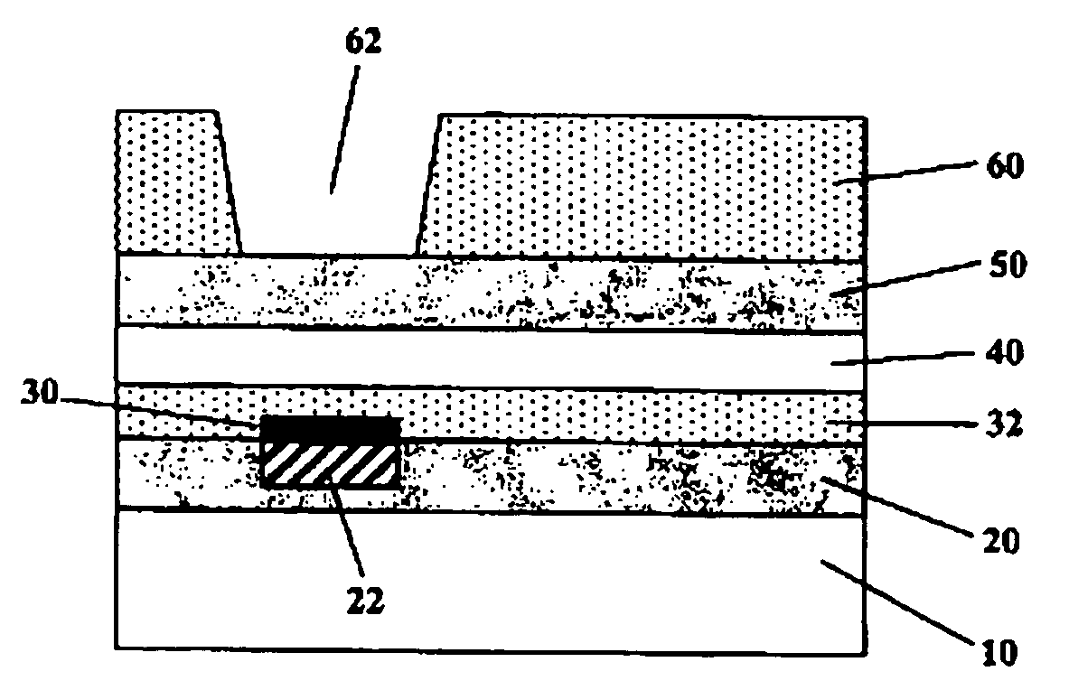
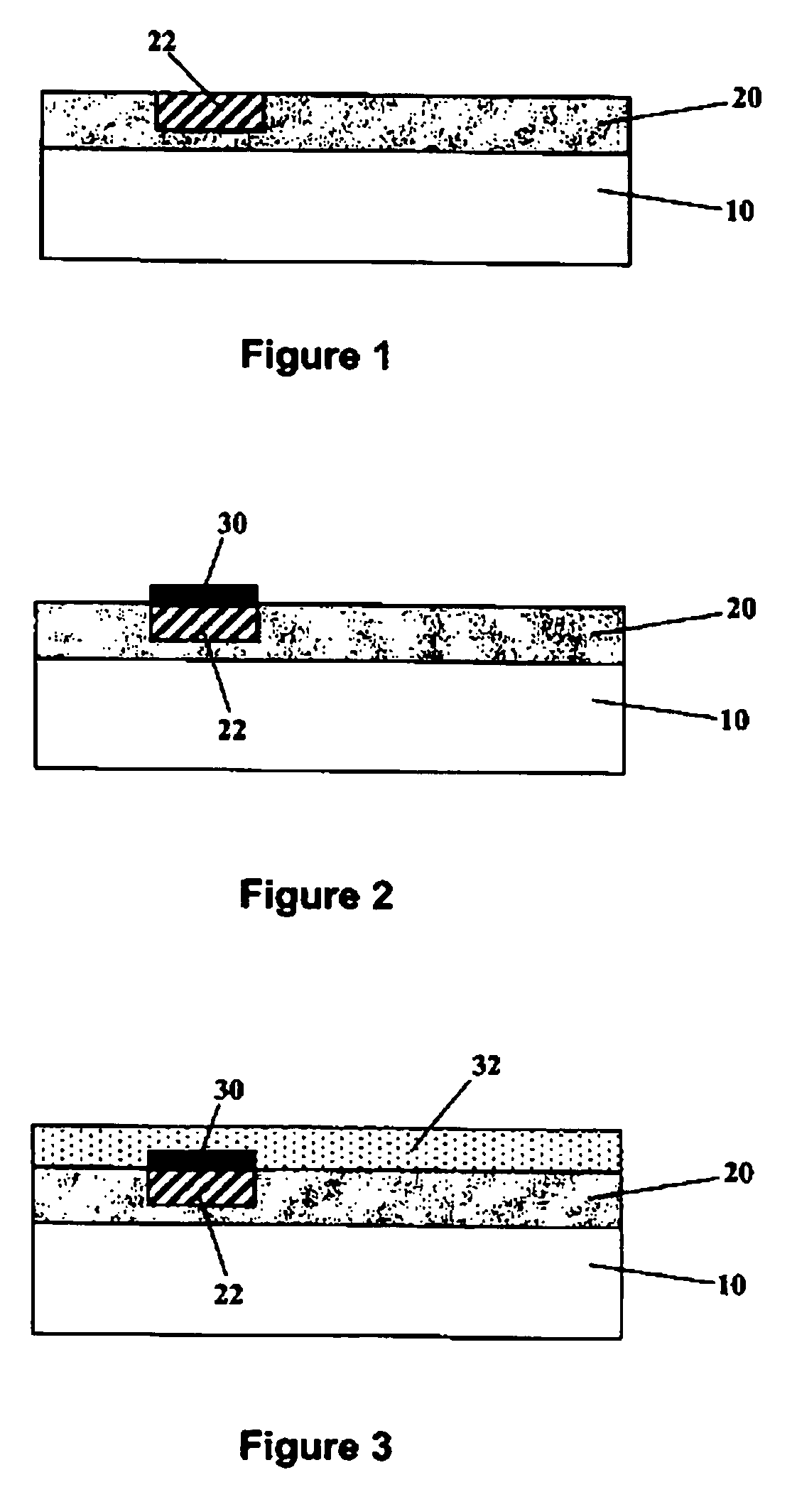
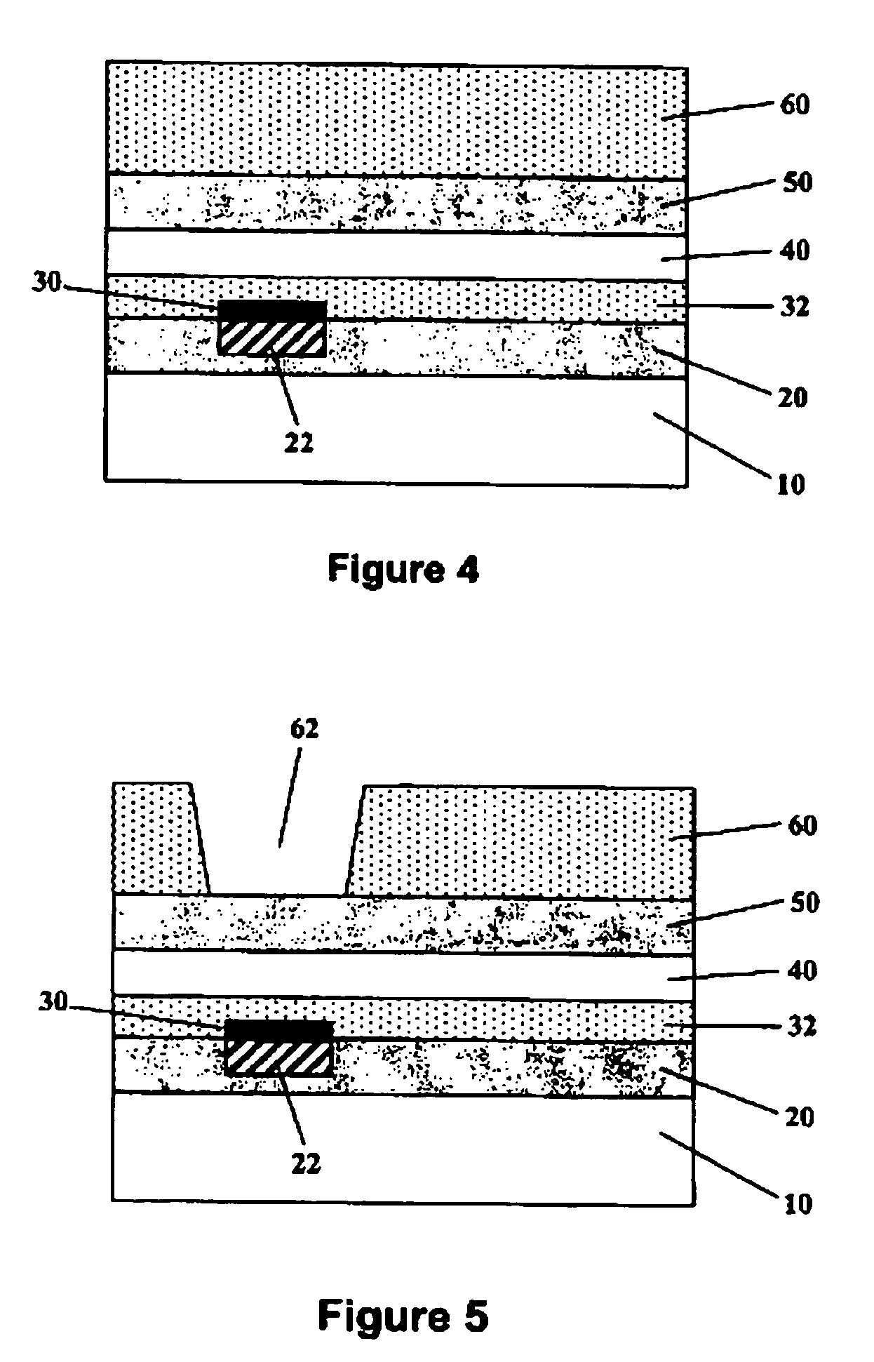
[0031]In the following description, numerous specific details are set forth, such as particular structures, components, materials, dimensions, processing steps and techniques, in order to provide a thorough understanding of the present invention. However, it will be appreciated by one of ordinary skill in the art that the invention may be practiced without these specific details. In other instances, well-known structures or processing steps have not been described in detail in order to avoid obscuring the invention.

[0032]It will be understood that when an element as a layer, region or substrate is referred to as being “on” another eleme...


PUM

PropertyMeasurementUnit
interfacial conductiveaaaaaaaaaa
conductiveaaaaaaaaaa
thicknessaaaaaaaaaa

Abstract

The present invention relates to a method for fabricating a semiconductor device with a last level copper-to-C4 connection that is essentially free of aluminum. Specifically, the last level copper-to-C4 connection comprises an interfacial cap structure containing CoWP, NiMoP, NiMoB, NiReP, NiWP, and combinations thereof. Preferably, the interfacial cap structure comprises at least one CoWP layer. Such a CoWP layer can be readily formed over a last level copper interconnect by a selective electroless plating process.

Description

FIELD OF THE INVENTION[0001]This invention relates to high-speed integrated circuit (IC) devices that contain conductive metallization. More specifically, the present invention relates to a method for fabricating an interfacial cap structure between the last level copper interconnect of an IC chip and a controlled-collapse chip connection (C4).BACKGROUND OF THE INVENTION[0002]In the fabrication of semiconductor devices, metal lines are often embedded in dielectric layers in a multilevel structure, particularly in the latter stage (“back end of the line” or “BEOL”) of the fabrication process. The last layer of metal lines (sometimes referred to in the art as the terminal via or TV layer) with metal pads formed thereon are fabricated by a process typically referred to as “far back end of line” or “FBEOL.” The pads and metal lines together provide last level interconnects from an IC chip to other system components. The majority of IC chips use aluminum (Al) to form the interconnects, b...

Claims


Application Information

Patent Timeline
Patent Type & Authority Applications(United States)
IPC IPC(8): H01L21/44
CPCH01L21/288H01L2224/0401H01L24/03H01L24/05H01L24/11H01L24/13H01L2224/05147H01L2224/05575H01L2224/05599H01L2224/1148H01L2224/13007H01L2224/13022H01L2224/13111H01L2924/01004H01L2924/01013H01L2924/01029H01L2924/01033H01L2924/01073H01L2924/01078H01L2924/01082H01L2924/04941H01L2924/14H01L2924/19041H01L2924/19042H01L2924/19043H01L23/3192H01L2924/01327H01L2924/00014H01L2924/014H01L2924/01075H01L2924/01074H01L2924/01042H01L2924/01006H01L2924/01005H01L2924/01015H01L2224/03009
Inventor DAUBENSPECK, TIMOTHY H.LANDERS, WILLIAM F.ZUPANSKI-NIELSEN, DONNA S.
Owner GLOBALFOUNDRIES INC
Features
  • R&D
  • Intellectual Property
  • Life Sciences
  • Materials
  • Tech Scout
  • Unparalleled Data Quality
  • Higher Quality Content
  • 60% Fewer Hallucinations
Learn More