[0010] The object of this invention is to solve the problem of the
conventional technique described above and provide a comparative
inspection method for comparing an inspection object image with a reference image and detecting an incoincident portion as a fault wherein the data is voted in a scattergram constituting one of multidimensional spaces at the time of brightness comparison, and the scattergram thus obtained is separated based on the features so that the data spread on each separated scattergram is suppressed thereby to make it possible to set a low threshold value. Specifically, the object of the invention is to provide a
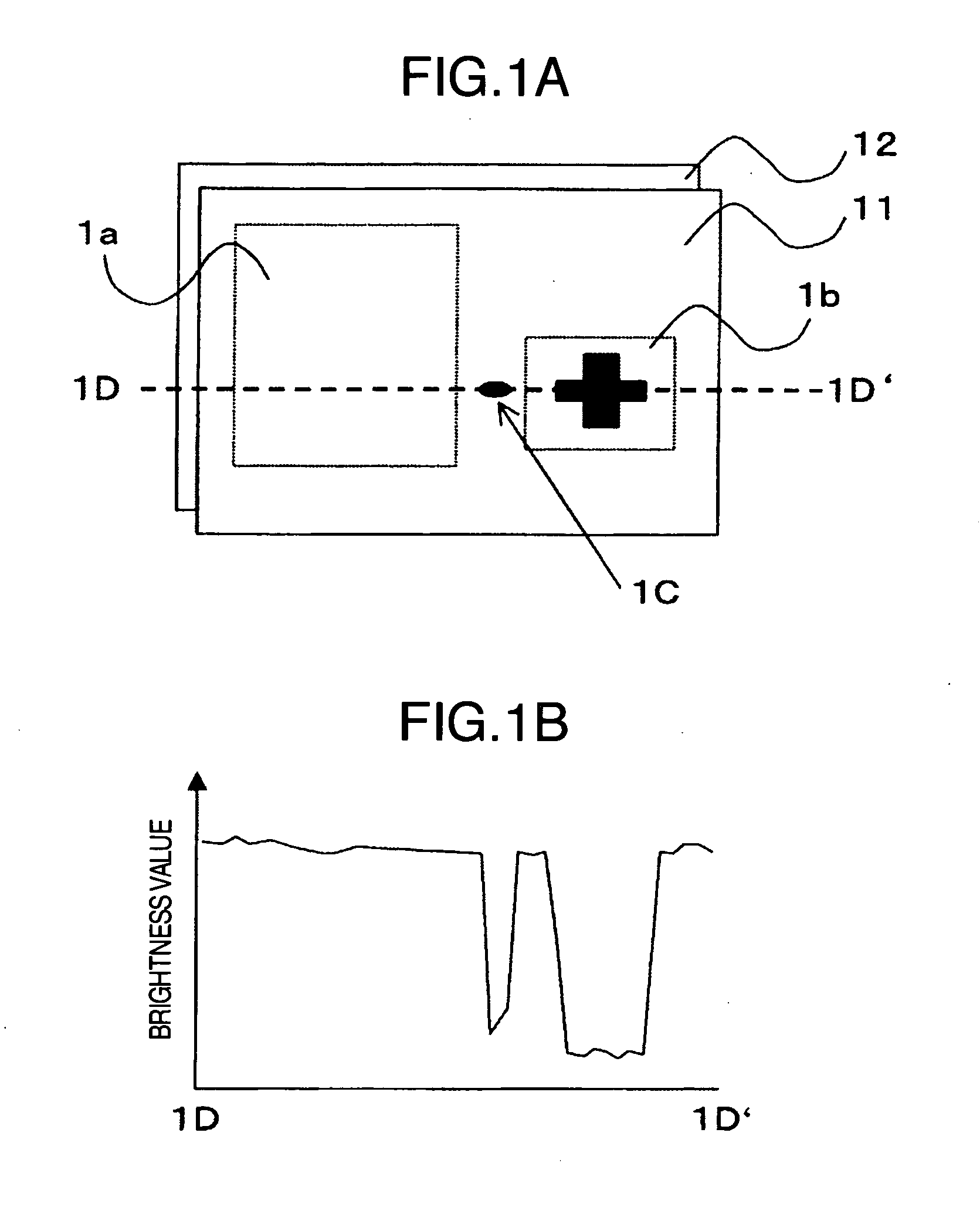
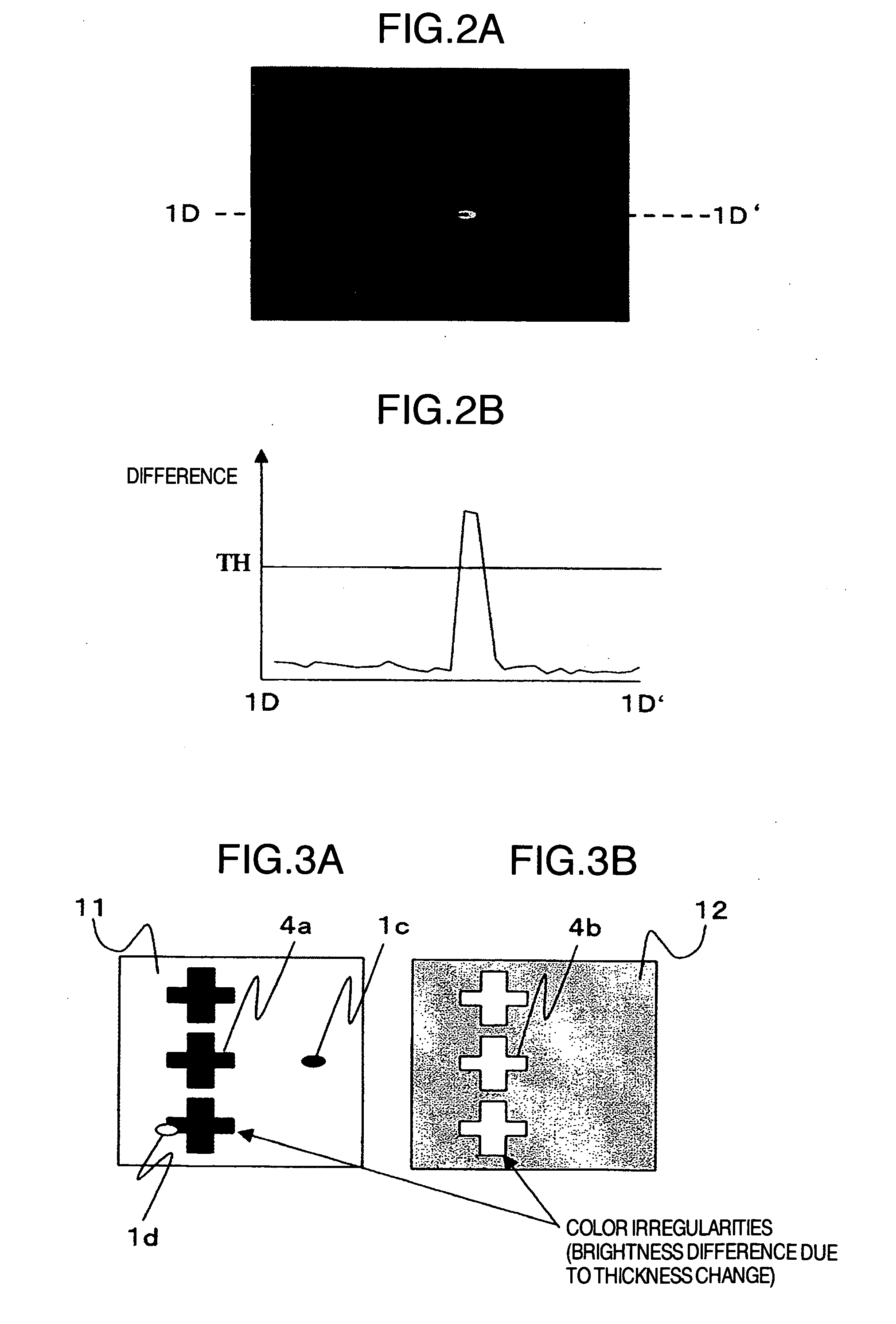
highly sensitive fault inspection method and apparatus, wherein the scattergram constituting one of the multidimensional spaces is plotted with the ordinate and the abscissa representing the brightness of the inspection object image and the brightness of the reference image, respectively, thereby reducing the false information due to the color shading (color irregularities), or in particular, wherein the pattern brightness irregularities caused by the thickness difference are inspected by combining the brightness between images in the semiconductor wafer inspection, so that the false information due to the brightness irregularities is reduced without increasing the threshold value TH thereby to realize a
highly sensitive fault inspection. Although a comparative inspection with the brightness as an object of comparison is explained, the ordinate and the abscissa of the scattergram represent the an object other than brightness in the case where such object is employed for comparison. Alternatively, three or more features are selected to form a multidimensional scattergram. As another alternative, the scattergram may be regarded as a given section of a
multidimensional space. The feature amounts selected include the brightness and contrast of the object image or the brightness variations of the corresponding pixels between chips (which are subsequently
cut into devices) or cells (repetitive patterns in the
chip). Further, a pattern inspection for detecting the fault desired by the user and buried in noises or requiring
no detection, with a high sensitivity by changing the sensitivity in accordance with the fault type.
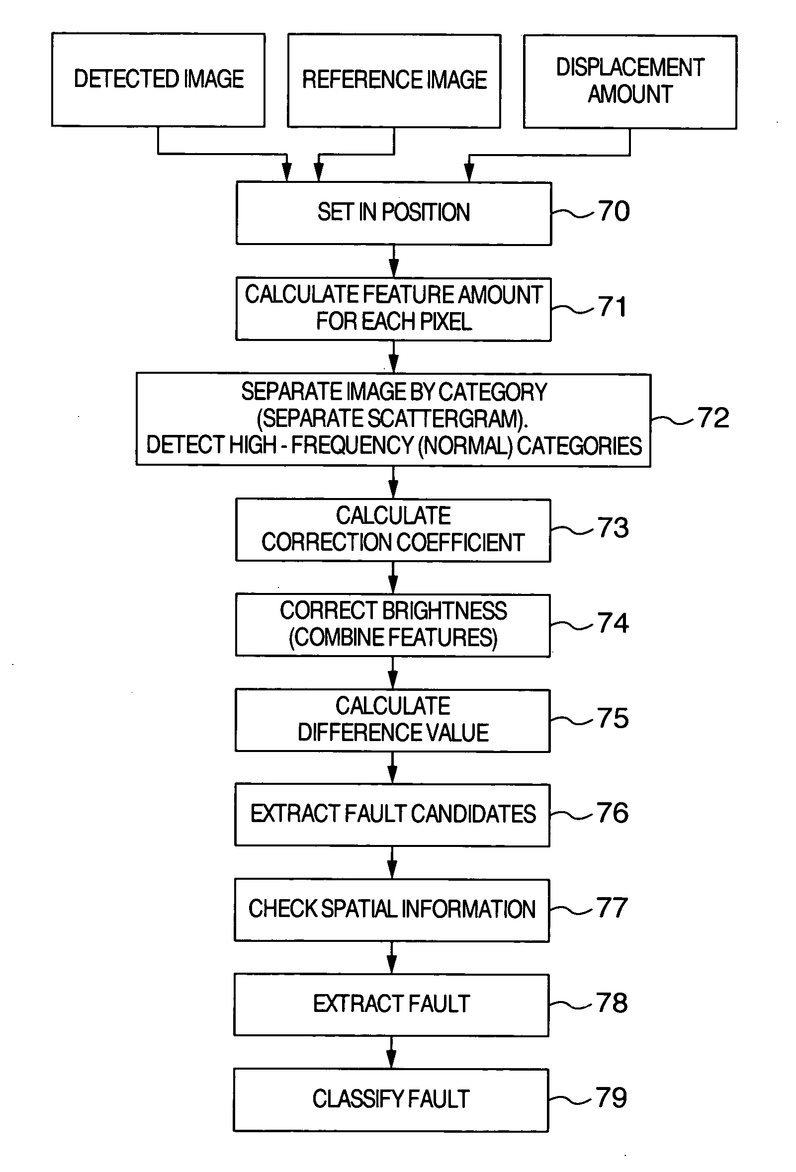
[0011] According to this invention, in comparing the inspection object image and the reference image with each other, the feature amounts including the brightness and contrast of each object pixel, the brightness or contrast variations between chips or cells are calculated and voted in a
multidimensional space having these features as axes, and a fault is detected using this voting data. As an example, an error value in the feature space is determined as a fault candidate, so that a high sensitivity pattern inspection adapted for a great variety of fault types can be carried out. Also, according to this invention, the feature space is formed by selected ones of a plurality of the feature amounts thereby to adjust the fault type detected. Also, the scattergram is created by voting, and the scattered diagram thus obtained is separated based on the features, while by suppressing the data spread on each scattergram separated, a low threshold value can be set.
[0012] Further, there is provided a fault inspection method wherein even in the case where the brightness difference is caused between the same patterns of the images due to the difference of the thickness of the object, a
highly sensitive fault inspection is possible with a low threshold value regardless of brightness irregularities by combining the brightness in advance. In general expression, a method employed for combining the object features such as brightness makes possible a highly sensitive inspection and reduce false information without being affected by the incoincidence of the normal portion. Specifically, the scattergram including some features such as the brightness or contrast variations of the object pixels or the brightness variation between dies or cells is separated by other features, and a fault is detected using a plurality of scattergrams separated.
[0014] Also, the user teaches the absence of a fault thereby to automatically set the threshold value for detecting the error value in such a manner as to cover all the distribution points in the feature space. As a result, the setting of the inspection conditions is simplified while at the same time making it possible to detect the matter other than taught as a fault with high sensitivity.
[0015] In addition, by increasing the teachings, the threshold value is optimized and the automatic sensitivity adjustment facilitated.

