Semiconductor device

a semiconductor chip and semiconductor technology, applied in semiconductor devices, semiconductor/solid-state device details, electrical devices, etc., can solve the problems of abnormally increasing the temperature of the semiconductor chip, the device is extremely susceptible to heating influence, and the automobile itself is used in a severe environment receiving repeated temperature increases and decreases

Inactive Publication Date: 2007-08-09
HITACHI LTD
View PDF7 Cites 2 Cited by
  • Summary
  • Abstract
  • Description
  • Claims
  • Application Information

AI Technical Summary

Benefits of technology

[0005] For the above problems, the inventors focused attention to the fact that heat from the semiconductor chip 1 at the time of energization of the semiconductor device is radiated from the lead electrode and the case electrode to the outside of the device, and found that what influences heat release capability on the heat radiating routes most is the joint areas of the joint members 2 and 6 facing the semiconductor chip 1 and that the influences of the joint areas of the joint members 4 and 8 located away from the semiconductor chip 1 are relatively small. Therefore, it is found that, in the semiconductor device, a desirable structure is such that a crack does not develop in the joint members 2 and 6 facing the semiconductor chip 1 even with repeated terminal impacts, and moreover the joint areas of the joint members 4 and 8 located away from the semiconductor chip 1 are ensured to some degree even if a crack develops therein.

Problems solved by technology

In addition, being mounted on an engine room of an automobile, the semiconductor device is extremely susceptible to an influence of heating at other electrical components mounted on the vehicle.
Moreover, the automobile itself is used under a severe environment receiving repeated temperature increases and decreases over a wide temperature range, such as temperature differences in midsummer.
Also, the areas of the heat radiating routes through the joint members 2, 4, and 6 are decreased to decrease heat release capability, thereby abnormally increasing the temperature of the semiconductor chip 1.
Eventually, the joint members 2, 4, and 6 are melted, and the semiconductor chip 1 reaches a heat-resistance limit, thereby causing a loss of the rectification function and also causing a failed state.

Method used


Image

  • Semiconductor device
  • Semiconductor device
  • Semiconductor device

Examples


first embodiment

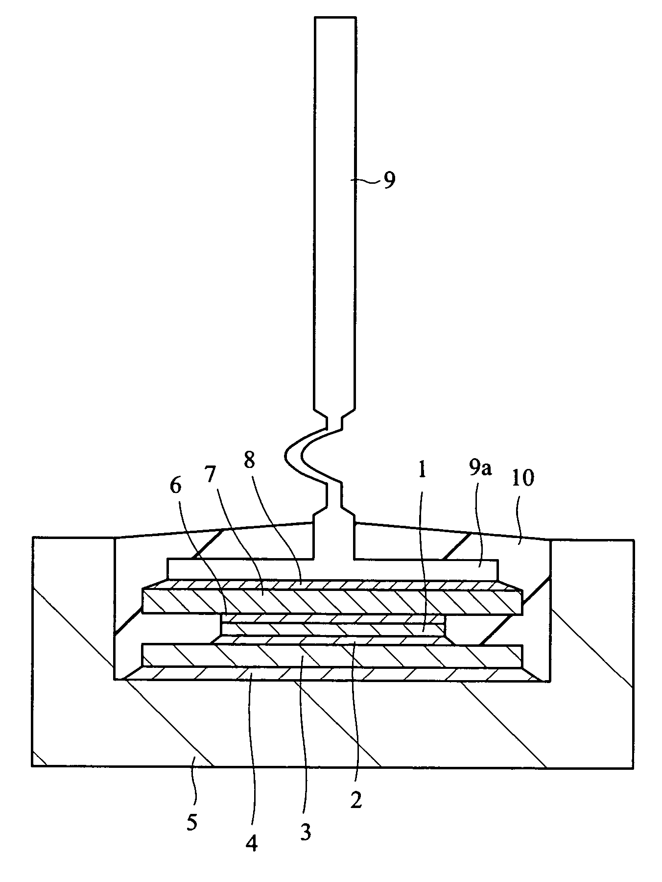
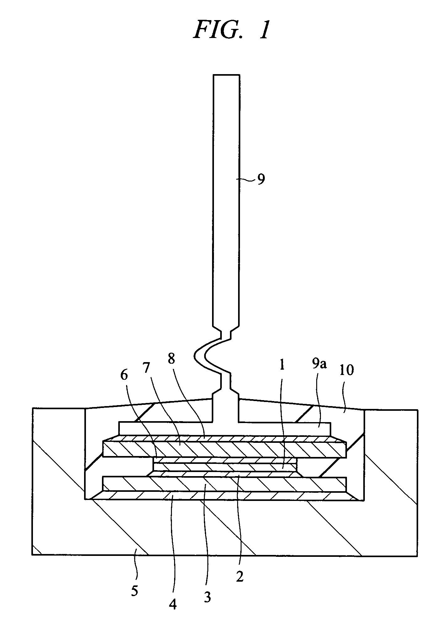
[0014] A first embodiment of the present invention is described with reference to FIG. 1. A semiconductor device shown in FIG. 1 includes a semiconductor chip 1, a stress relief member 3 which is a second conductive member disposed via a joint member 2 (solder) on a lower surface side of the semiconductor chip 1, a case electrode 5 disposed via a joint member 4 on a further lower side of the stress relief member 3 on the lower surface side of the semiconductor chip 1, a stress relief member 7 which is a first conductive member disposed via a joint member 6 on an upper side of the semiconductor chip 1, a lead electrode 9 having a header portion of lead electrode 9a disposed via a joint member 8 on a further upper surface side of a stress relief member 7 on the upper surface side of the semiconductor chip 1, the header portion of lead electrode 9a having a diameter larger than the lead for the purpose of bonding with the joint member.

[0015] The semiconductor chip has a rectification ...

second embodiment

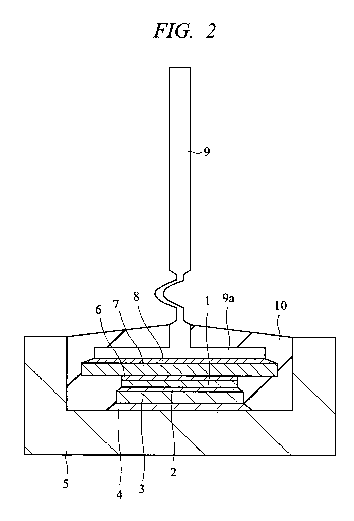
[0025] A second embodiment of the present invention is described with reference to FIG. 2. FIG. 2 depicts an example of structure in which, in a semiconductor device including a semiconductor chip 1, a stress relief member 3 disposed via a joint member 2 on a lower surface side of the semiconductor chip 1, a case electrode 5 disposed via a joint member 4 on a further lower side of the stress relief member 3 on the lower surface side of the semiconductor chip 1, a stress relief member 7 disposed via a joint member 6 on an upper side of the semiconductor chip 1, and a lead electrode 9 having a header portion of lead electrode 9a disposed via a joint member 8 on a further upper surface side of the stress relief member 7 on the upper surface side of the semiconductor chip 1, the header portion of lead electrode 9a having a diameter larger than a lead for the purpose of bonding with the joint member, the stress relief member 7 on the upper surface side of the semiconductor chip 1 and the...


PUM


Abstract

By making coefficients of linear thermal expansion of stress relief members on upper and lower surface sides of a semiconductor chip small, thermal strain on joint members above and below the semiconductor chip is decreased and development of a crack therein is suppressed to ensure a joint area. Furthermore, by making areas of electrodes and stress relief members large enough to include a project plane of the semiconductor chip projected onto the joint surfaces thereof, even if a crack develops into the joint member between the stress relief member and the electrode, a joint area larger than the area of the semiconductor chip can be ensured for a certain amount of time. As a result, a semiconductor device capable of simultaneously ensuring the joint areas of the respective joint members and preventing a decrease in heat release capability is provided.

Description

CROSS-REFERENCE TO RELATED APPLICATION [0001] The present application claims priority from Japanese Patent Application No. JP 2006-030393 filed on Feb. 8, 2006, the content of which is hereby incorporated by reference into this application. TECHNICAL FIELD OF THE INVENTION [0002] The present invention relates to a vehicle-mounted semiconductor device for converting an alternating current to a direct current. BACKGROUND OF THE INVENTION [0003] The device according to the present invention is a vehicle-mounted semiconductor device mounted on an alternating-current generator of an automobile and having a rectification function of converting an alternating current output to a direct current output. FIG. 6 is a cross-sectional view of a state of mounting of a conventional vehicle-mounted semiconductor device. In FIG. 6, 1 denotes a semiconductor chip, 2 denotes a joint member that joins the semiconductor chip 1 and a stress relief member 3 together, 3 denotes the stress relief member for...

Claims


Application Information

Patent Timeline
Patent Type & Authority Applications(United States)
IPC IPC(8): H01L23/48
CPCH01L23/051H01L23/24H01L2924/01074H01L23/492H01L24/01H01L24/33H01L2924/01013H01L2924/01029H01L2924/01082H01L2924/01006H01L2924/01033H01L2924/01042H01L2924/0105H01L2924/3512H01L2924/00H01L2924/181
Inventor HIRAMITSU, SHINJIMATSUYOSHI, SATOSHISASAKI, KOJITERASAKI, TAKESHI
Owner HITACHI LTD
Why Eureka
Try Eureka