

Apparatus and method for manufacturing semiconductor device
- Summary
- Abstract
- Description
- Claims
- Application Information
AI Technical Summary
Benefits of technology
Problems solved by technology
Method used
Image

Examples
embodiment mode 2
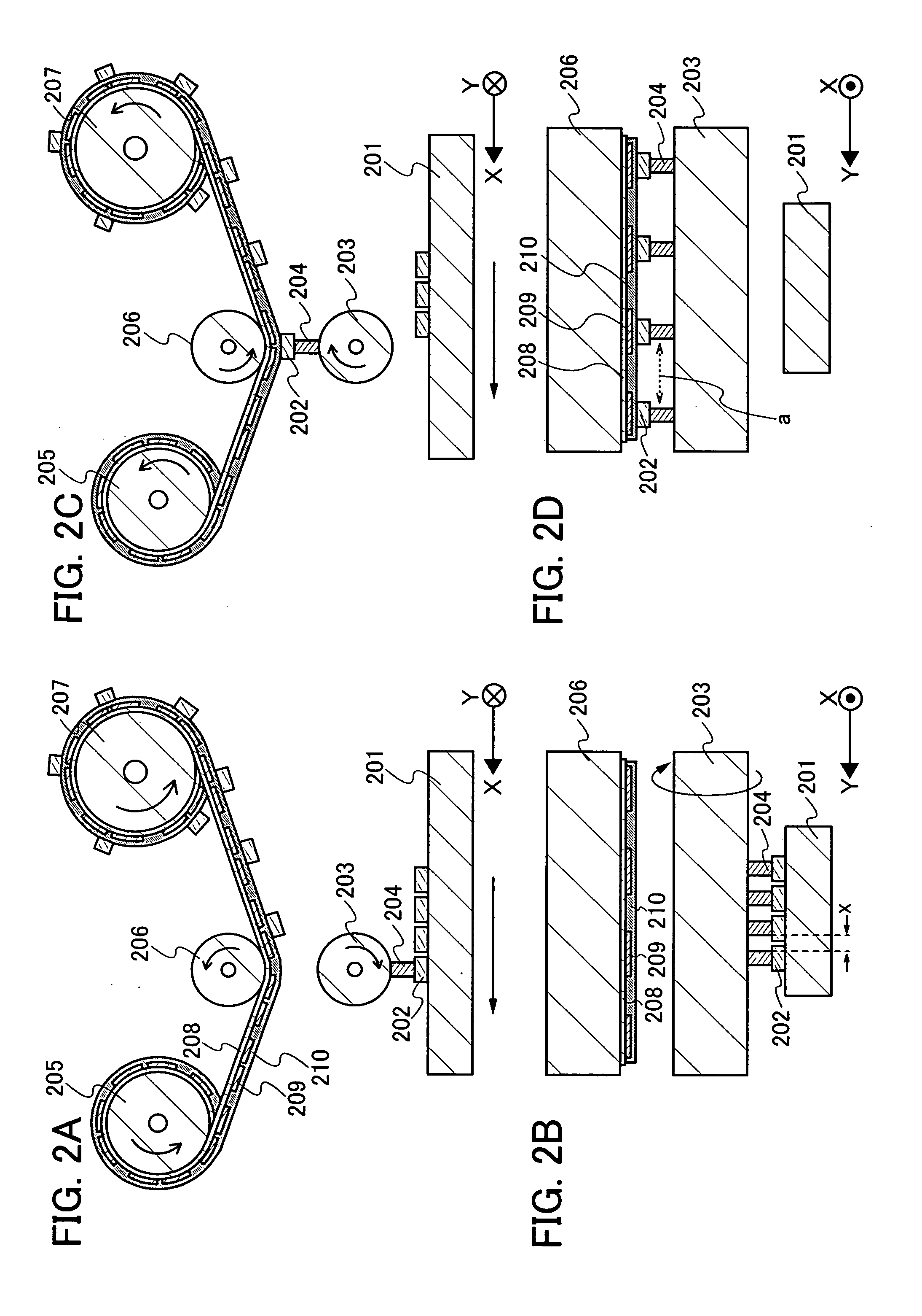
[0083]In this embodiment mode, an apparatus and a method for manufacturing a semiconductor device which employs a roll-to-roll system is described, with reference to FIGS. 2A to 2D, 3A to 3D, 4A to 4D and 19.
[0084]As shown in FIG. 19, a manufacturing apparatus of a semiconductor device in this embodiment mode includes a supply roller 205 around which a flexible substrate 208 having antennas 209 is wound, a roller 206 which controls the movement of the flexible substrate 208 and mounts semiconductor integrated circuits 202 on the respective antennas 209, and a collecting roller 207 for winding up the flexible substrate 208 having the antennas 209 on which the semiconductor integrated circuits 202 are mounted. The manufacturing apparatus also includes a support means 201 for supporting the semiconductor integrated circuits 202 and a roller 203 having holders 204 for catching and holding the semiconductor integrated circuits 202. Note that the holders 204 are arranged in a row on the s...
embodiment mode 3
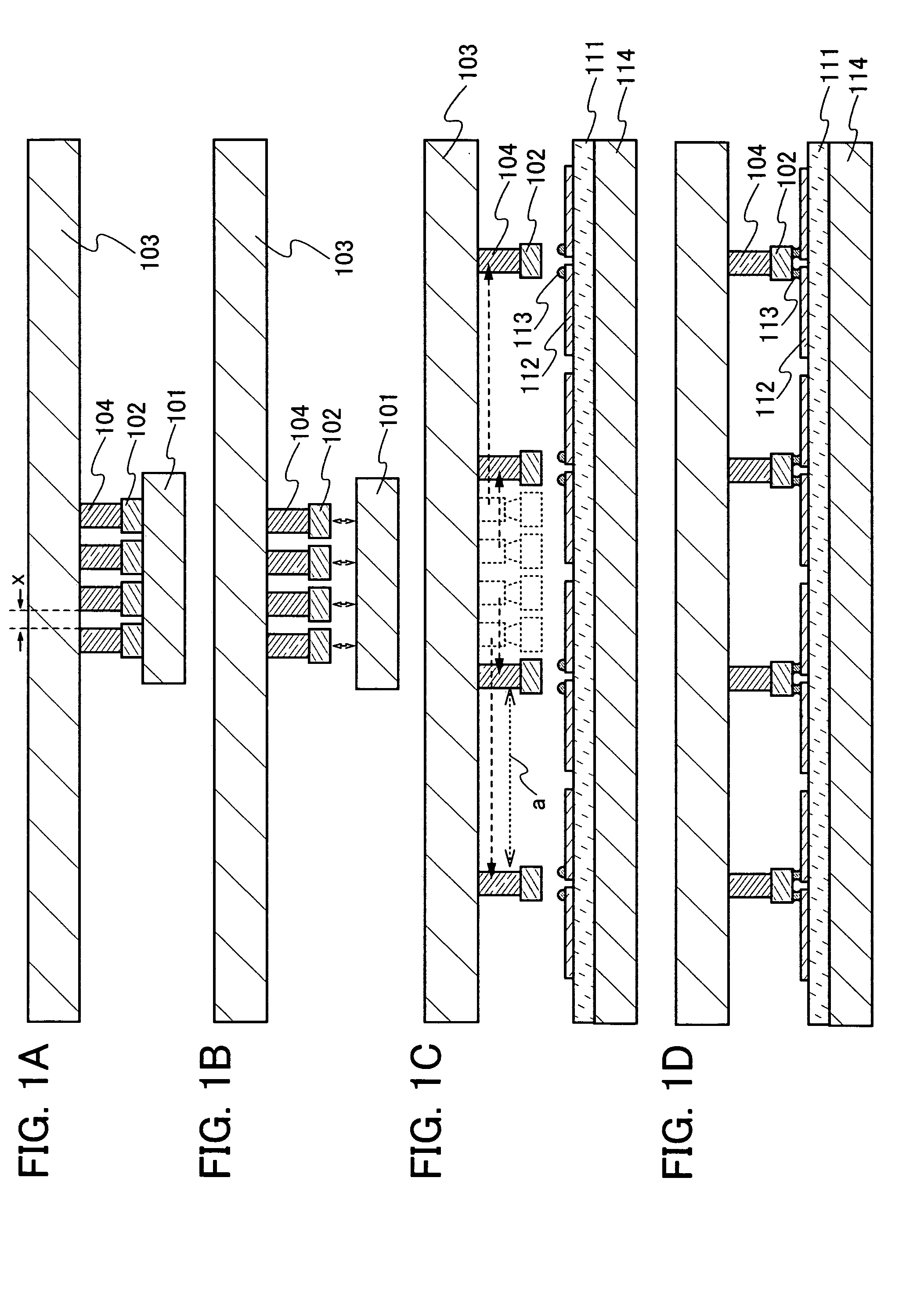
[0115]In this embodiment mode, examples of a manufacturing method of a semiconductor device is described with reference to FIGS. 5A and 5B, and 6A to 6C, which vary depending on which surface of the semiconductor integrated circuit over the support means 201 is provided with connection terminals. Note that in this embodiment mode, although description will be made by using the manufacturing apparatus of a semiconductor device shown in FIGS. 2A to 2D, the manufacturing apparatuses of a semiconductor device shown in FIGS. 3A to 4D can also be used as appropriate.
[0116]FIGS. 5A and 5B show cross sections of a manufacturing apparatus of a semiconductor device in the x-axis direction, similarly to FIGS. 2A and 2C. Although not shown in FIGS. 5A and 5B, a plurality of holders are arranged in a row in the y-axis direction of the roller, similarly to FIGS. 2B and 2D. Similarly, FIGS. 6A to 6C show cross sections of a manufacturing apparatus of a semiconductor device in the x-axis direction ...
embodiment mode 4
[0138]In this embodiment mode, a jig which is applicable to Embodiment Mode 2 or 3 is described with reference to FIGS. 7A, 7B, 8A and 8B.
[0139]A manufacturing apparatus of a semiconductor device shown in FIGS. 7A and 7B has a jig in which a roller 241 is provided with 2n (n is natural number) sets of holders. In FIGS. 7A and 7B, a jig in which the roller 241 is provided with two sets of holders 242a and 242b is shown. A pair of the holders 242a and 242b are preferably provided to be symmetrical about the rotation axis of the roller 241. As a result, a row of semiconductor integrated circuits over the support means 201 can be picked up, while at the same time another row of semiconductor integrated circuits can be attached to the flexible substrate 208 having antennas during a rotation of 1 / 2n. Therefore, throughput can be improved.
[0140]Here, by rotating the rollers 206 and 241 in opposite directions or in the same direction, semiconductor integrated circuits 202a over the support ...
PUM
| Property | Measurement | Unit |
|---|---|---|
| Flexibility | aaaaa | aaaaa |
Abstract
Description
Claims
Application Information