Transforming metrology data from a semiconductor treatment system using multivariate analysis

a technology of metrology data and semiconductor treatment system, applied in the field of multivariate analysis of metrology data, can solve the problems of limiting the size and resolution of the library of simulated diffraction signals that can be generated, time and computational capacity needed and the inability to generate simulated diffraction signals

Active Publication Date: 2007-08-09
TOKYO ELECTRON LTD
View PDF2 Cites 48 Cited by
  • Summary
  • Abstract
  • Description
  • Claims
  • Application Information

AI Technical Summary

Problems solved by technology

However, the process of generating a simulated diffraction signal typically involves performing a large number of complex calculations, which can be time consuming and computationally intensive.
The amount of time and computational capability and capacity needed to generate simulated diffraction signals can limit the size and resolution (i.e., the number of entries and the increment between entries) of the library of simulated diffraction signals that can be generated.
Moreover, the complexity of the measured diffraction signals (i.e., the amount of data) and the potential for the existence of noise can further hinder accurate correlation between measured diffraction signals and simulated diffraction signals.

Method used


Image

  • Transforming metrology data from a semiconductor treatment system using multivariate analysis
  • Transforming metrology data from a semiconductor treatment system using multivariate analysis
  • Transforming metrology data from a semiconductor treatment system using multivariate analysis

Examples


Embodiment Construction

[0024] The following description sets forth numerous specific configurations, parameters, and the like. It should be recognized, however, that such description is not intended as a limitation on the scope of the present invention, but is instead provided as a description of exemplary embodiments.

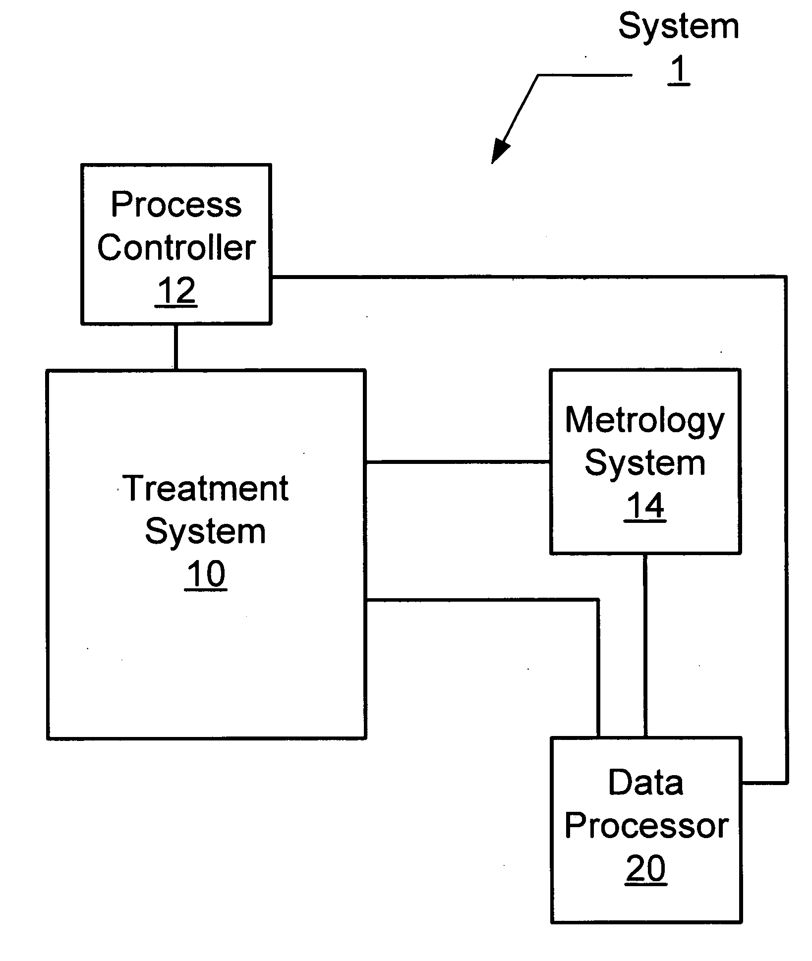
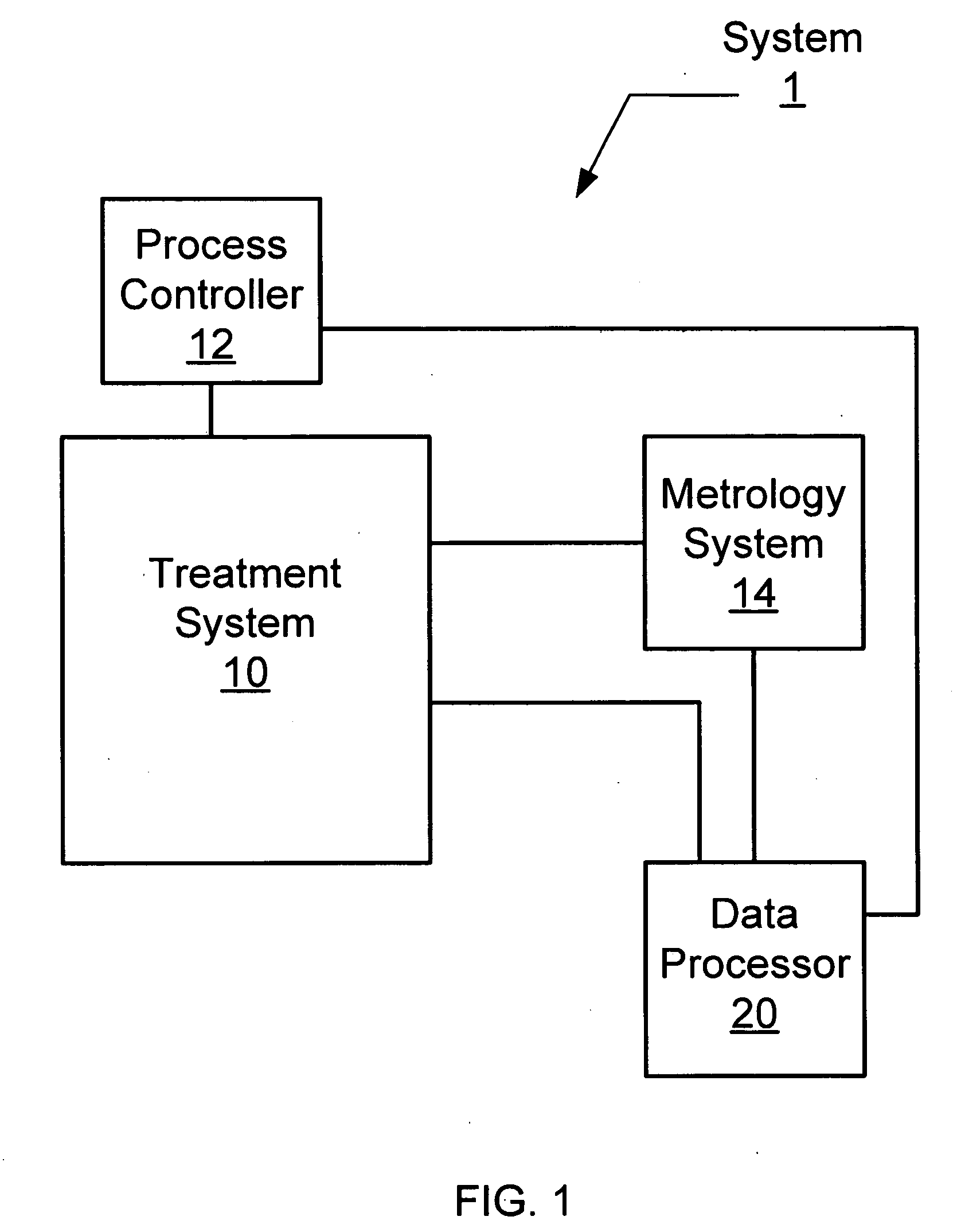
[0025] Referring now to the drawings, wherein like reference numerals designate identical or corresponding parts throughout the several views, FIG. 1 illustrates a material processing system 1 comprising a semiconductor treatment system 10 configured to treat a substrate, a process controller 12 for performing at least one of monitoring, measuring, adjusting, or controlling, or a combination of two or more thereof, process data for performing a treatment process in treatment system 10. Process data include values of process variables in the treatment process such temperature and time for a treatment process. Material processing system 1 further comprises a metrology system 14 for measuring ...


PUM


Abstract

Metrology data from a semiconductor treatment system is transformed using multivariate analysis. In particular, a set of metrology data measured or simulated for one or more substrates treated using the treatment system is obtained. One or more essential variables for the obtained set of metrology data is determined using multivariate analysis. A first metrology data measured or simulated for one or more substrates treated using the treatment system is obtained. The first obtained metrology data is not one of the metrology data in the set of metrology data earlier obtained. The first metrology data is transformed into a second metrology data using the one or more of the determined essential variables.

Description

BACKGROUND [0001] 1. Field [0002] The present application relates to transforming metrology data from a semiconductor treatment system, and, more particularly, to transforming metrology data using multivariate analysis. [0003] 2. Related Art [0004] In semiconductor manufacturing, metrology is increasingly utilized to ensure that individual process steps, as well as a sequence of process steps, adhere to design specifications. For example, metrology may be employed to identify instances of process drift, and provide data sufficient to establish control schemes for correcting such drift. [0005] While critical dimension scanning electron microscopy (CD-SEM) metrology has been used in the past, the complexity of devices formed on semiconductor substrates and their ever-decreasing feature size (e.g., sub 100 nm technology nodes), coupled with increasingly sophisticated unit process and process integration schemes, have warranted the implementation of optical metrology. In addition to bei...

Claims


Application Information

Patent Timeline
Patent Type & Authority Applications(United States)
IPC IPC(8): G06F15/00
CPCG01N21/211G01N2021/215G01N21/4788G06F17/40G06F15/00
Inventor VUONG, VIBAO, JUNWEICHEN, YANHEIKO, WEICHERTEGRET, SEBASTIEN
Owner TOKYO ELECTRON LTD
Why Eureka
Try Eureka