
Transition circuit

a technology of transition circuit and circuit body, applied in waveguides, electrical equipment, antennas, etc., can solve the problems of increasing the thickness of the circuit structure, deteriorating the performance of the transition circuit itself, and the wiring cannot be carried out at all in the portion, so as to reduce the thickness

Active Publication Date: 2007-08-16
MITSUBISHI ELECTRIC CORP
View PDF10 Cites 12 Cited by
  • Summary
  • Abstract
  • Description
  • Claims
  • Application Information

AI Technical Summary

Benefits of technology

[0014] There is obtained an effect that the transition circuit can have a reduced thickness by having this construction without the need for providing a particular hollow under its dielectric substrate.

Problems solved by technology

In the conventional transition circuit, there is a problem that the hollow is formed beneath the dielectric substrate projecting through the notched portion into the waveguide, thereby increasing the thickness in the circuit construction.
Moreover, there is a problem that if a multilayer dielectric substrate is used, wiring can not be carried out at all in the portion thereof which is inserted into the waveguide.
Further, there is a problem that when a through hole is made through the dielectric substrate and further, the notched portion of the waveguide sandwiches the substrate between the upper part and the lower part of the portion in order to construct the transition circuit, the occurrence of a misalignment between the positions of the upper and lower inner walls of the waveguide deteriorates the performance of the transition circuit itself.

Method used


Image

  • Transition circuit
  • Transition circuit
  • Transition circuit

Examples


embodiment 1

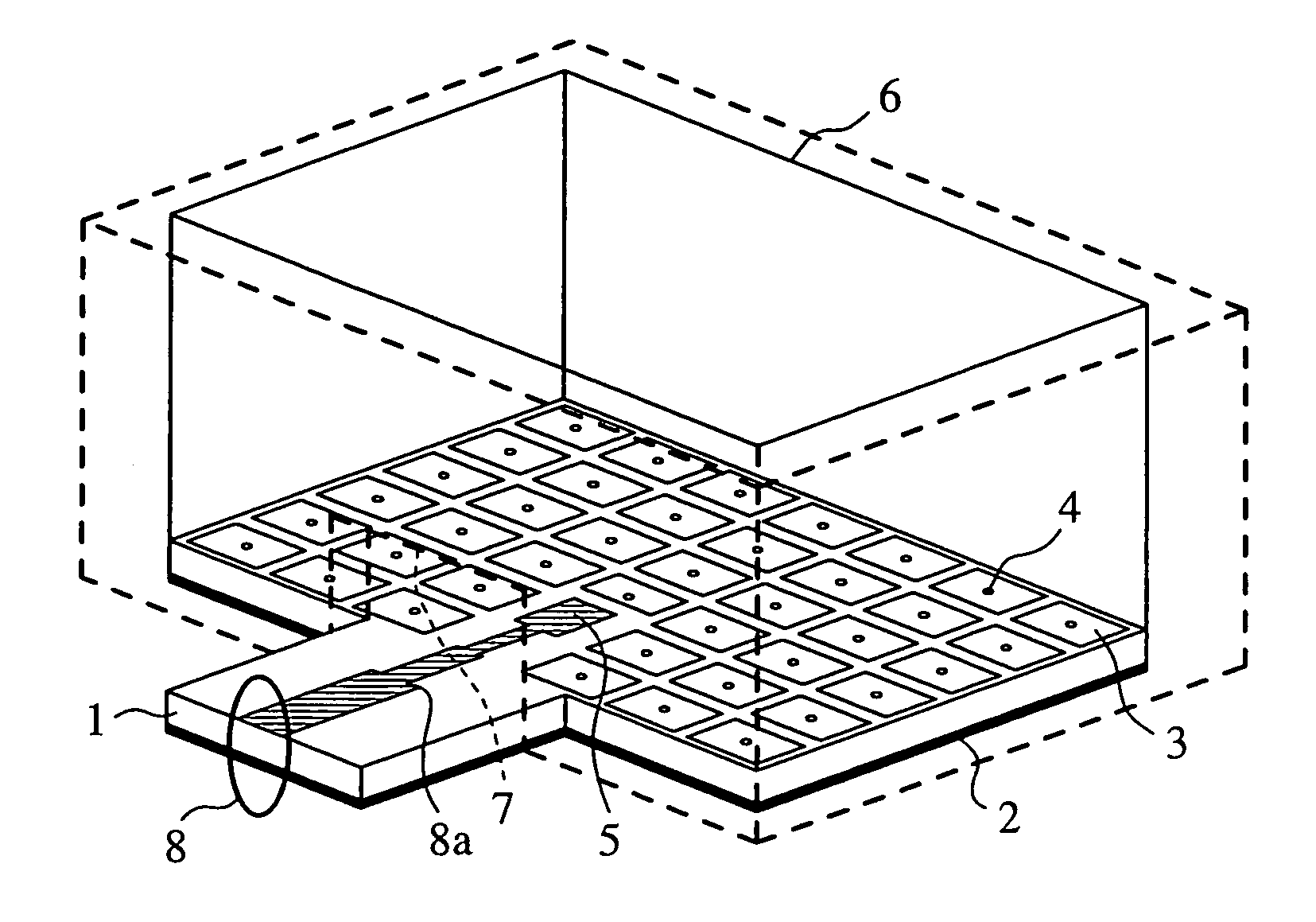
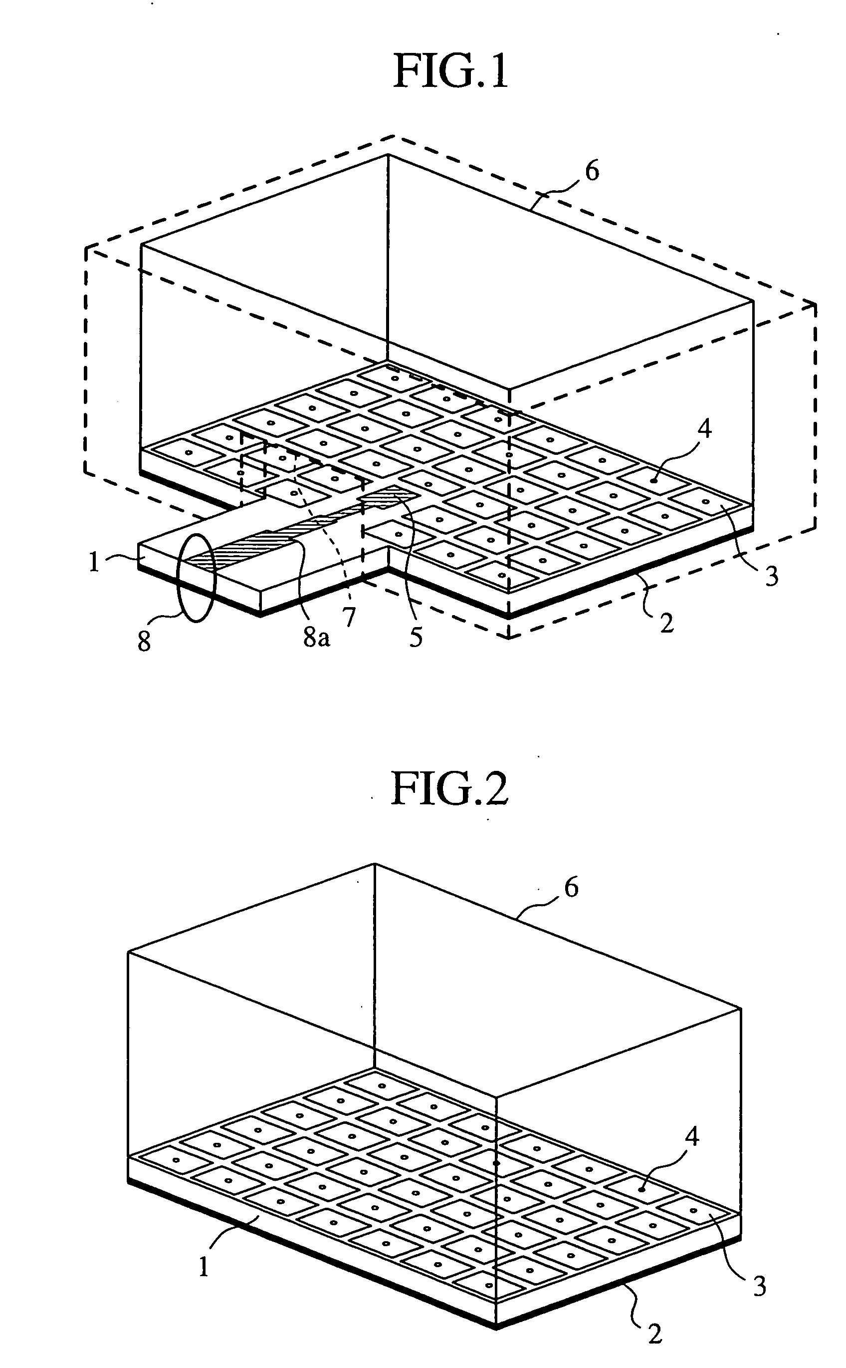
[0030]FIG. 1 is a view showing the construction of a transition circuit in accordance with Embodiment 1 of the present invention. Referring to the figure, a dielectric substrate 1 includes two conductor layers. A ground conductor 2 is the first conductor layer of the dielectric substrate 1. In the second conductor layer of the dielectric substrate 1, are regularly disposed a plurality of polygonal conductor patterns 3. In this embodiment, the conductor pattern is a square one.

[0031] The ground conductor 2, which is the first conductor layer of the dielectric substrate 1 and each of the polygonal conductor patterns 3, which are formed in the second conductor layer thereof, are electrically connected through a through hole (electrical connection portion) 4. An open stub 5 is formed flush with the conductor layer, in which the plurality of polygonal conductor patterns 3 are disposed, on the dielectric substrate 1, and the stub has a rectangular shape the width of which is changed in t...

embodiment 2

[0053] In Embodiment 1, the example in which the transition circuit is constructed by use of two conductor layers formed on the dielectric substrate 1 is shown. In Embodiment 2, the dielectric substrate having three or more conductor layers is used to construct the transition circuit with two conductor layers arbitrarily selected therefrom. This construction can increase flexibility in the arrangement of layers in the dielectric substrate.

[0054]FIG. 5 is a view showing the construction of a transition circuit in accordance with Embodiment 2 of the present invention. In accordance with Embodiment 2, a multilayer substrate having three conductor layers therein is used for the dielectric substrate 1. The ground conductor 2 is formed in the first conductor layer, and the open stub 5 and the conductor patterns 3 are formed in the third conductor layer, which is the top layer.

[0055] In the second conductor layer disposed between the first conductor layer and the third conductor layer in...

embodiment 3

[0067] In Embodiment 2, the example is shown in which the microwave transmission line 8 consists of the conductor 8a formed on the top face of the extending portion of the dielectric substrate 1, the ground conductor 2 formed in the first conductor layer on the dielectric substrate 1, and the second ground conductor 11.

[0068] In Embodiment 3, a new dielectric substrate is placed over the conductor 8a and the open stub 5 formed on the dielectric substrate 1. Further, on the top face of the dielectric substrate, which is newly laminated thereto, a new second ground conductor 13 is provided at the position where the second ground conductor is symmetrical to the ground conductor 2 formed on the dielectric substrate 1 with the conductor 8a formed on the dielectric substrate 1 as a reference plane. This ground conductor 13 and the ground conductor 2 are electrically connected by a plurality of through holes 11 to construct the microwave transmission line 8.

[0069]FIG. 6 is a view showing...


PUM


Abstract

A transition circuit includes: a waveguide having a notched portion formed by cutting away a portion of the tube wall of the waveguide from the end portion of the waveguide; a dielectric substrate in which a portion extending outside the waveguide through the notched portion of the waveguide is formed; a plurality of polygonal conductor patterns formed regularly disposed on the dielectric substrate; a ground conductor formed on the dielectric substrate; through holes electrically connecting this ground conductor and each of the conductor patterns; an open stub formed on the dielectric substrate; and the conductor of a microwave transmission line, which is formed on the portion of the dielectric substrate, extending outside the waveguide, and which is electrically connected to the open stub.

Description

TECHNICAL FIELD [0001] The present invention relates to a transition circuit converting the transmission path of a high frequency such as a microwave or a millimeter wave from a waveguide to a microwave transmission line coupled thereto that is formed on a dielectric substrate. BACKGROUND ART [0002] For a transition circuit between a waveguide and a microwave transmission line formed on a dielectric substrate, there is a transition circuit as described in JP-A-6-140816, for example. With this transition circuit, a constructional example of a waveguide and a microstripline is shown. [0003] In the conventional device described in the above literature, the dielectric substrate on which an open stub is formed is inserted into the waveguide through a notched portion formed by removing a portion of the side of the waveguide. At that time, the dielectric substrate is inserted thereinto such that a hollow is formed between the lower side of the dielectric substrate and the end face of the w...

Claims


Application Information

Patent Timeline
Patent Type & Authority Applications(United States)
IPC IPC(8): H01P5/107H01Q15/00
CPCH01Q15/008H01P5/107
Inventor OHNO, ARAKIOHHASHI, HIDEYUKITAHARA, YUKIHIROKODAMA, KATSUHISA
Owner MITSUBISHI ELECTRIC CORP
Learn More