
Semiconductor integrated circuit device

Active Publication Date: 2007-08-16
MITSUMI ELECTRIC CO LTD
View PDF44 Cites 4 Cited by
  • Summary
  • Abstract
  • Description
  • Claims
  • Application Information

AI Technical Summary

Benefits of technology

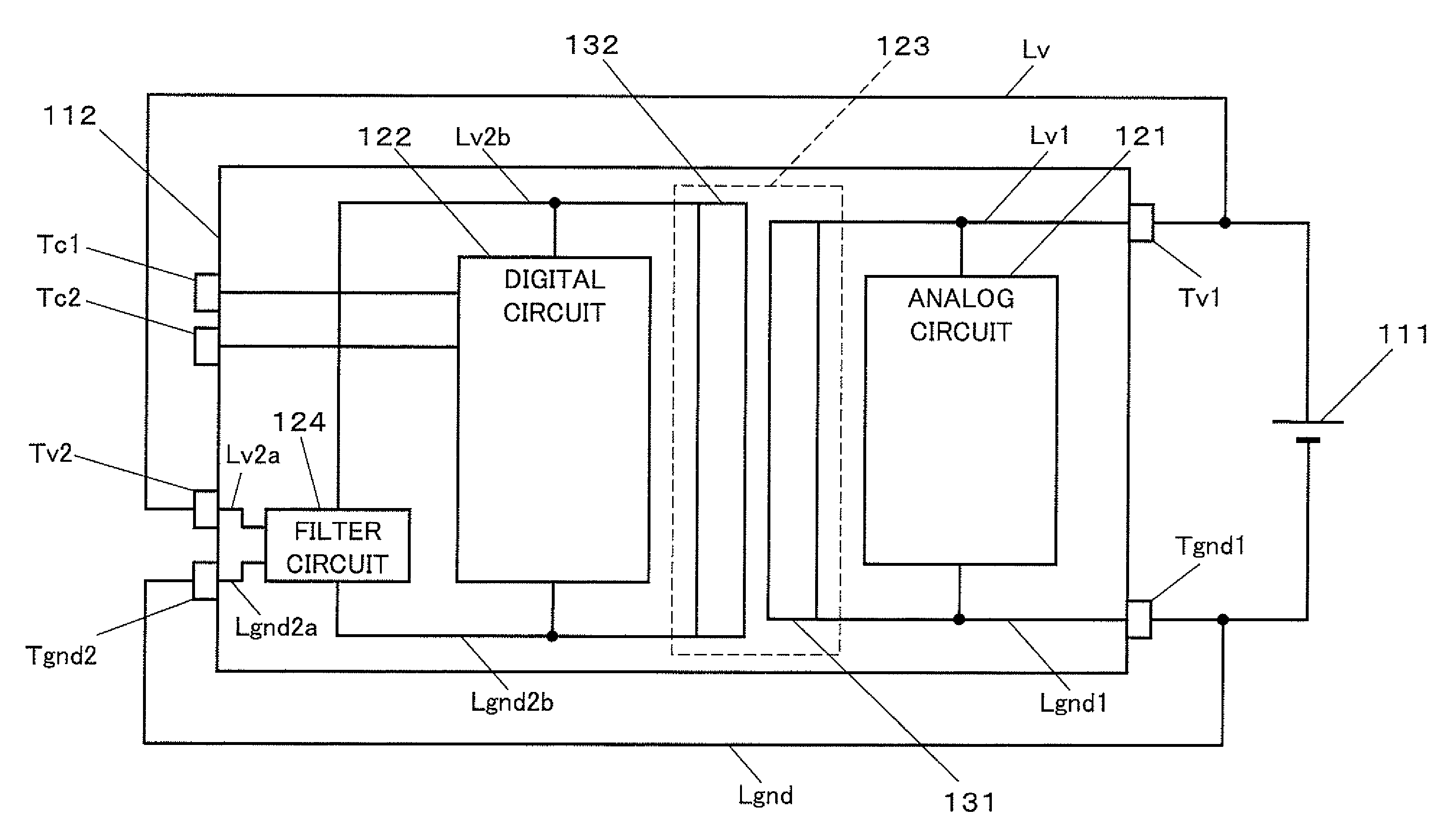
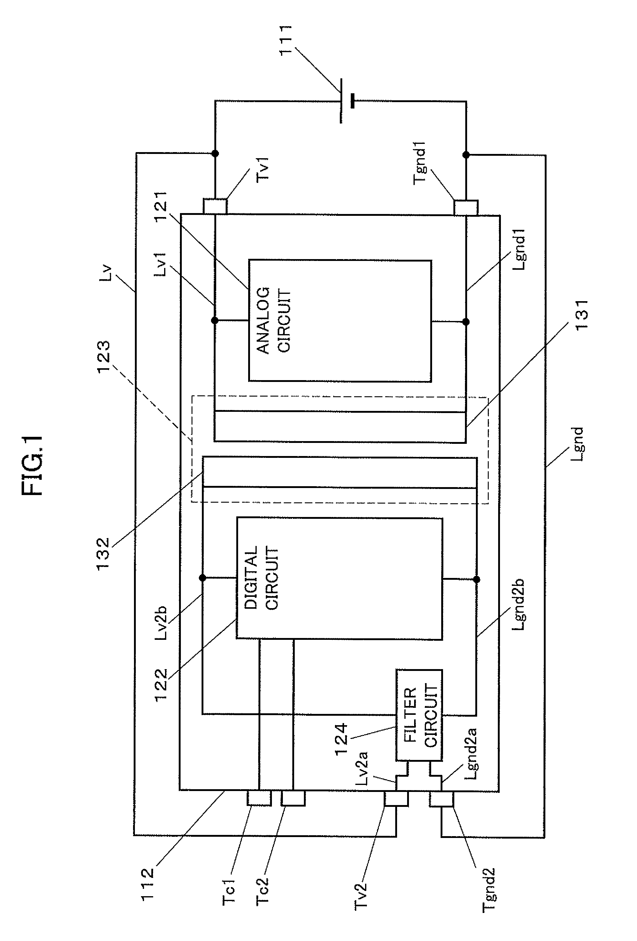
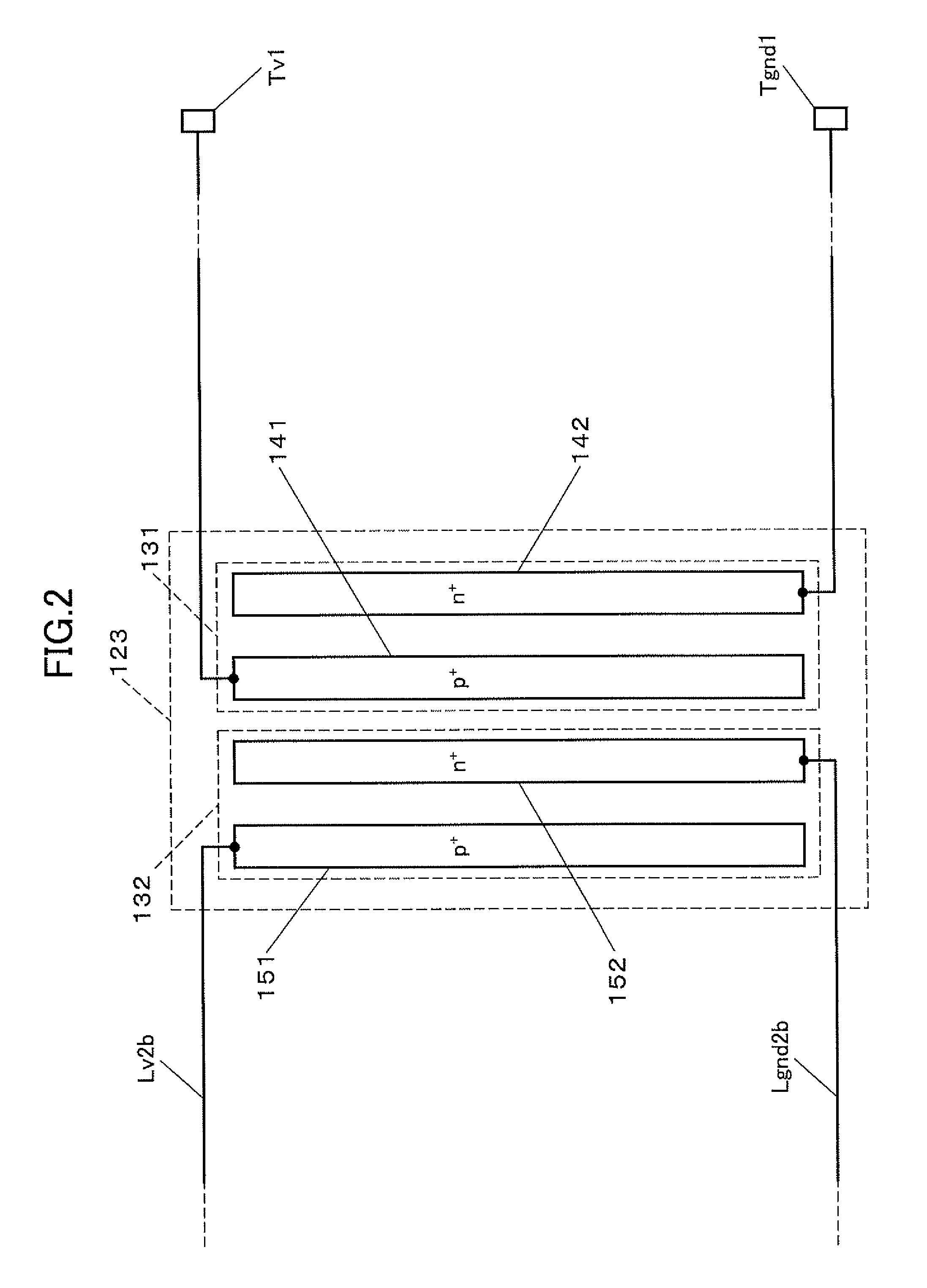
[0012]An embodiment of the present invention provides a semiconductor integrated circuit device including a digital circuit and an analog circuit formed on one semiconductor substrate; a guard band formed on the semiconductor substrate in a position between the digital circuit and the analog circuit and configured to prevent noise generated in the digital circuit from being transmitted to the analog circuit; a first power supply terminal positioned on a periphery of the semiconductor substrate near the analog circuit and configured to supply a power-supply voltage to the analog circuit; a first ground terminal positioned on the periphery of the semiconductor substrate near the analog circuit and configured to supply a ground potential to the analog circuit; a second power supply terminal positioned on the periphery of the semiconductor substrate near the digital circuit and configured to supply the power-supply voltage to the digital circuit; a second ground terminal positioned on the periphery of the semiconductor substrate near the digital circuit and configured to supply the ground potential to the digital circuit; and a filter circuit positioned between the second power supply terminal, the second ground terminal, and the digital circuit and configured to remove the noise transmitted from the digital circuit.
[001

Problems solved by technology

One problem in using a lithium ion battery is that it is generally difficult to measure the remaining battery power based on its voltage.
The noise generated in the digital circuits is transmitted within the one-chip semiconductor integrated circuit device to the analog circuits and, for example, reduces the resolution of A / D conversion.
Downsizing fuel gauge ICs increases the influence of noise and makes it difficult to provide a circuit or an electronic part used for noise reduction as an internal component.
This is a problem not only for fuel gauge ICs, but also for any semiconductor integrated circuit device including an analog circuit and a digital circuit.

Method used


Image

  • Semiconductor integrated circuit device
  • Semiconductor integrated circuit device
  • Semiconductor integrated circuit device

Examples


Embodiment Construction

[0026]Preferred embodiments of the present invention are described below with reference to the accompanying drawings.

[0027][Configuration of Fuel Gauge IC According to an Embodiment]

[0028]FIG. 1 is a block diagram illustrating an exemplary configuration of a fuel gauge IC provided as an example of a semiconductor integrated circuit device according to an embodiment of the present invention.

[0029]A fuel gauge IC 112 is formed on a single semiconductor substrate and includes an analog circuit 121, a digital circuit 122, a guard band 123, and a filter circuit 124. Along the periphery of the semiconductor substrate where the fuel gauge IC 112 is formed, a power supply terminal Tv1 and a ground terminal Tgnd1 for the analog circuit 121, a power supply terminal Tv2 and a ground terminal Tgnd2 for the digital circuit 122, and communication terminals Tc1 and Tc2 are provided.

[0030]The analog circuit 121 and the digital circuit 122 are placed apart from each other in the fuel gauge IC 112. T...


PUM


Abstract

A disclosed semiconductor integrated circuit device includes a digital circuit and an analog circuit formed on one semiconductor substrate; a guard band configured to prevent noise generated in the digital circuit from being transmitted to the analog circuit; a first power supply terminal configured to supply a power-supply voltage to the analog circuit; a first ground terminal configured to supply a ground potential to the analog circuit; a second power supply terminal configured to supply the power-supply voltage to the digital circuit; a second ground terminal configured to supply the ground potential to the digital circuit; and a filter circuit positioned between the second power supply terminal, the second ground terminal, and the digital circuit and configured to remove the noise transmitted from the digital circuit.

Description

BACKGROUND OF THE INVENTION[0001]1. Field of the Invention[0002]The present invention generally relates to a semiconductor integrated circuit device, and more particularly relates to a semiconductor integrated circuit device including a digital circuit and an analog circuit.[0003]2. Description of the Related Art[0004]Currently, lithium ion batteries are commonly used in portable devices such as digital cameras. One problem in using a lithium ion battery is that it is generally difficult to measure the remaining battery power based on its voltage. For this reason, the remaining battery power of a lithium ion battery is calculated, for example, by measuring and totaling the amounts of charge-and-discharge currents of the lithium ion battery with, for example, a microprocessor (patent document 1).[0005]For example, fuel gauge ICs are used for measuring remaining battery power as described above. A fuel gauge IC includes, for example, analog circuits such as a high-resolution A / D conve...

Claims


Application Information

Patent Timeline
IPC IPC(8): H03M1/12
CPCH01L21/761H01L23/585H01L23/64H03H7/075H01L2924/0002H03H2001/0085H01L2924/00
Inventor ITAGAKI, TAKATOSHI
Owner MITSUMI ELECTRIC CO LTD
Learn More