Semiconductor device having a trench gate and method of fabricating the same

Inactive Publication Date: 2007-08-16
NAN YA TECH
View PDF5 Cites 44 Cited by
  • Summary
  • Abstract
  • Description
  • Claims
  • Application Information

AI Technical Summary

Benefits of technology

[0007]Thus, an improved semiconductor device having a trench gate and a method of fabricating the capabl

Problems solved by technology

This method, however, may result in the short channel effect, significantly affecting the performance of semiconductor devices such as MOS transistors.
Control of the thick oxide having a predetermined thickness,

Method used


Image

  • Semiconductor device having a trench gate and method of fabricating the same
  • Semiconductor device having a trench gate and method of fabricating the same
  • Semiconductor device having a trench gate and method of fabricating the same

Examples


Embodiment Construction

[0017]The following description is of the best-contemplated mode of carrying out the invention. This description is made for the purpose of illustrating the general principles of the invention and should not be taken in a limiting sense. The scope of the invention is best determined by reference to the appended claims.

[0018]In this specification, expressions such as “overlying the substrate”, “above the layer”, or “on the film” simply denote a relative positional relationship with respect to the surface of a base layer, regardless of the existence of intermediate layers. Accordingly, these expressions may indicate not only the direct contact of layers, but also, a non-contact state of one or more laminated layers.

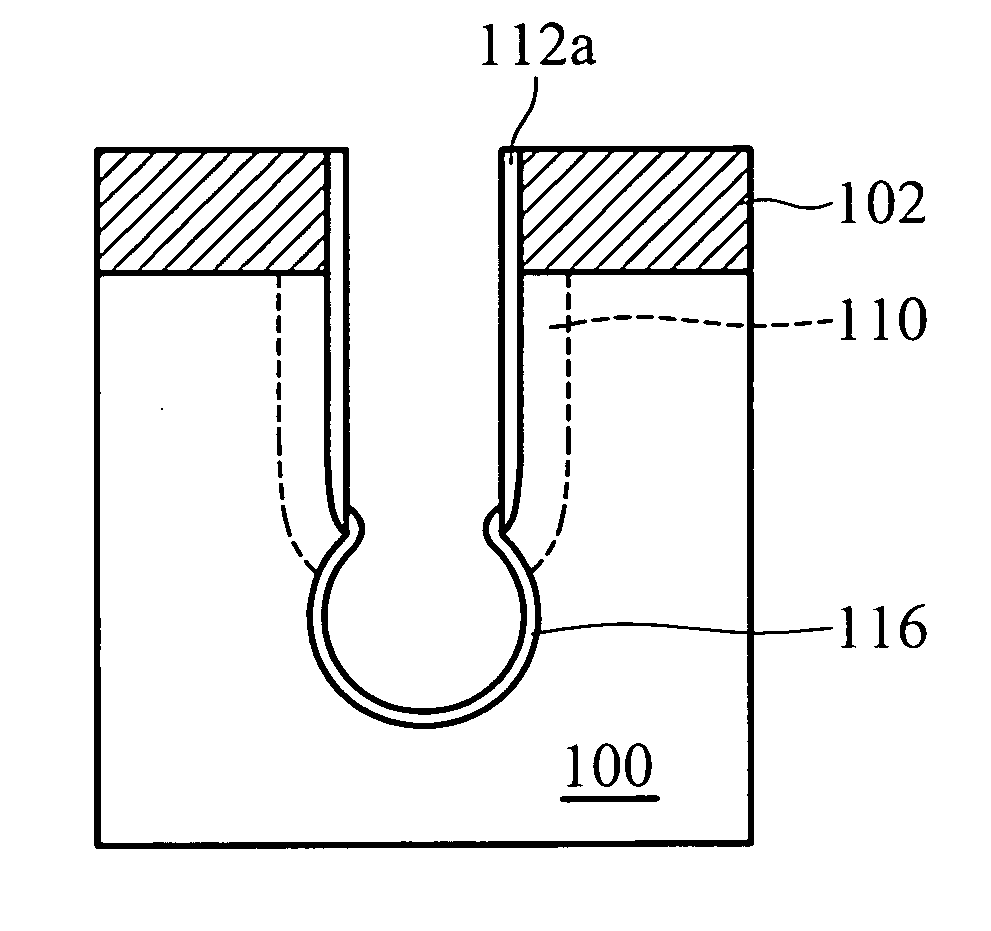
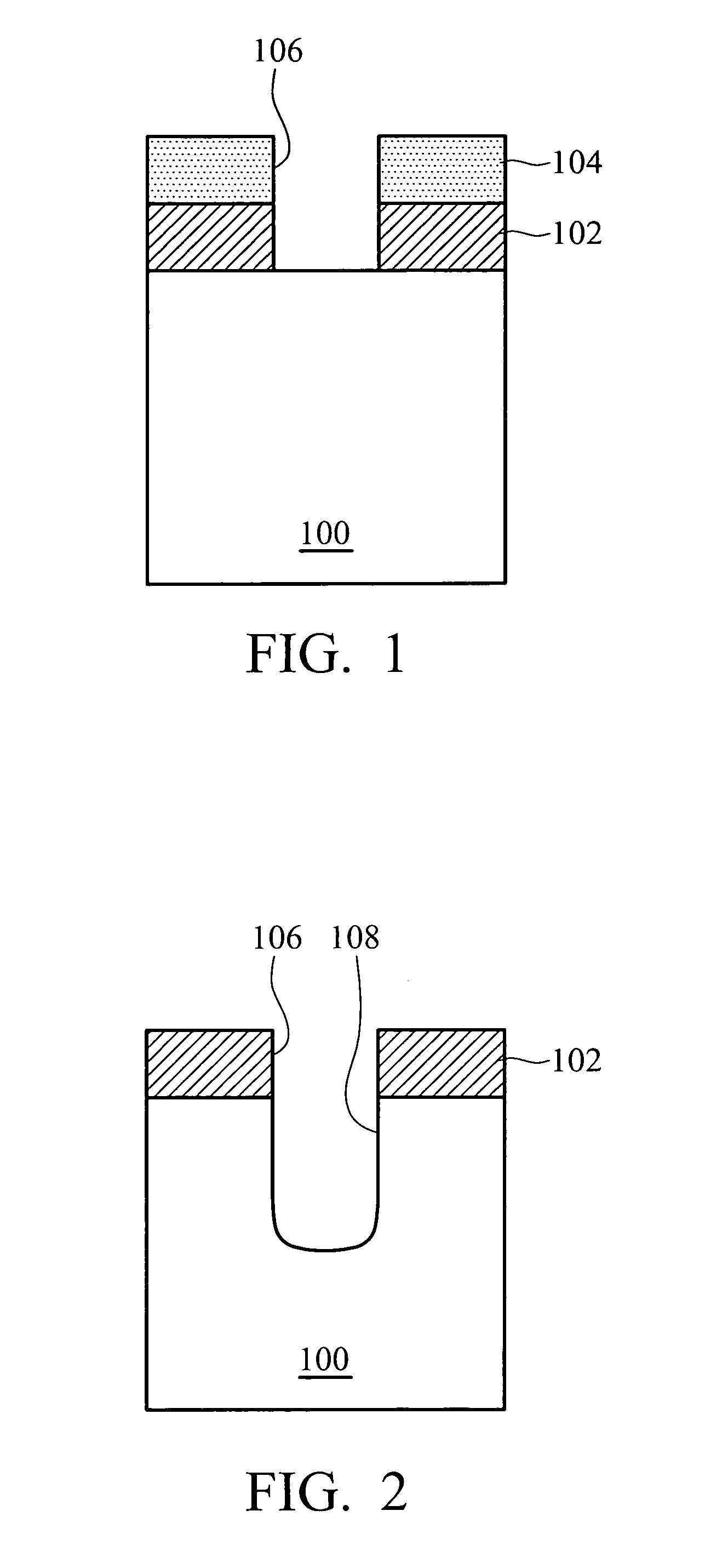
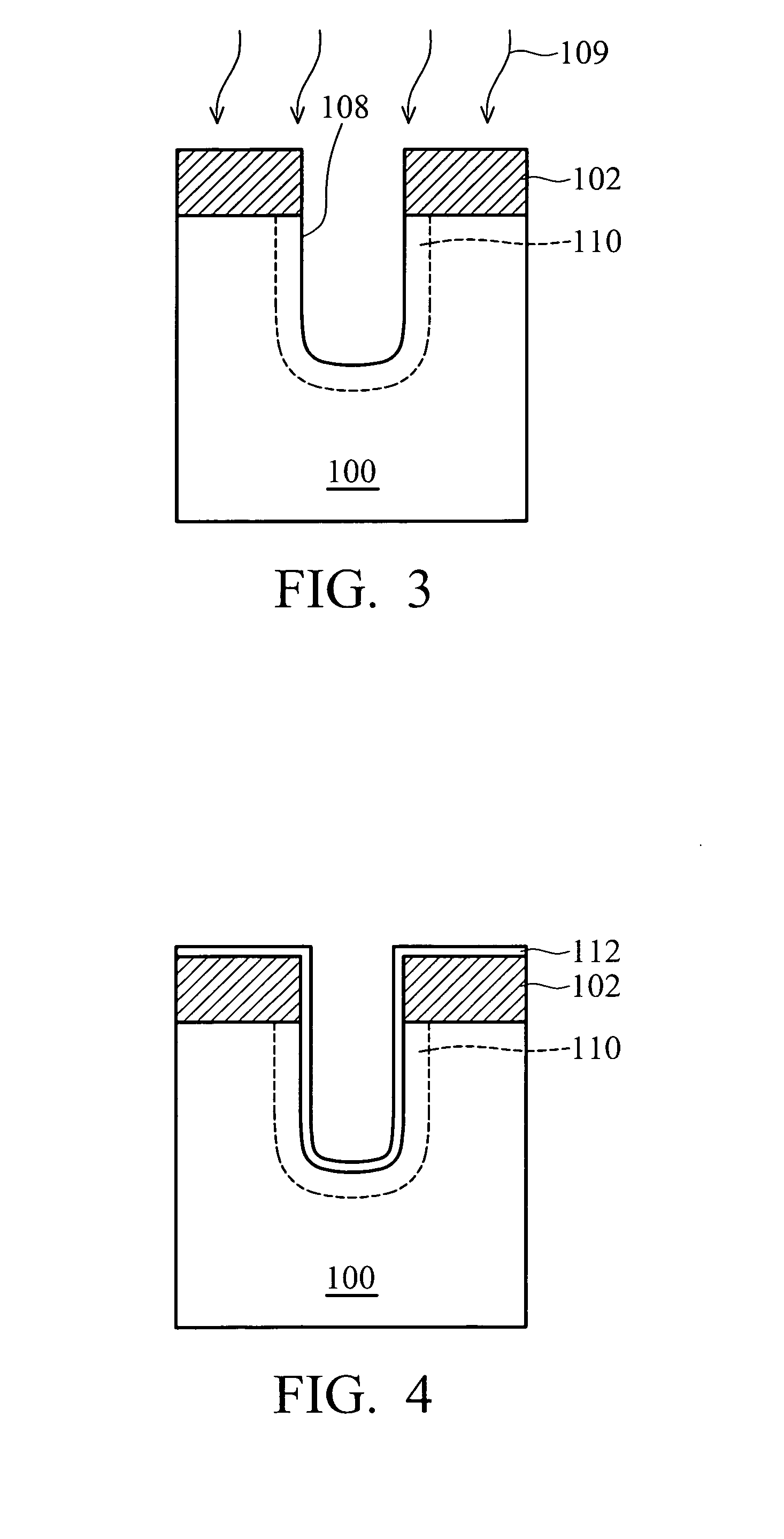
[0019]FIGS. 1 to 8 are cross sections of an exemplary process flow of manufacturing a semiconductor device having a trench gate.

[0020]As shown in FIG. 1, a semiconductor substrate 100 is provided. The semiconductor substrate 100 may comprise silicon, gallium arsenide, galli...


PUM


Abstract

A method of fabricating a semiconductor device having a trench gate is provided. First, a semiconductor substrate having a trench etch mask thereon is provided. The semiconductor substrate is etched to form a trench having a sidewall and a bottom using the trench etch mask as a shield. Impurities are doped into the semiconductor substrate through the trench to form a doped region. The semiconductor substrate underlying the trench is etched to form an extended portion. A gate insulating layer is formed on the trench and the extended portion. A trench gate is formed in the trench and the extended portion.

Description

BACKGROUND OF THE INVENTION[0001]1. Field of the Invention[0002]The invention relates to semiconductor fabrication, and more particularly relates to a metal oxide semiconductor transistor (MOS transistor) having a trench gate and a method of fabricating the same.[0003]2. Description of the Related Art[0004]Continuous development of semiconductor devices has resulted in devices, such as MOS transistors, capable of high performance, high integration and high operating speed. Continued integration demands that the size of MOS transistors on a semiconductor substrate must continuously be reduced. Higher integration of MOS transistors can be achieved, for example, by reducing gate length and / or source / drain region size. This method, however, may result in the short channel effect, significantly affecting the performance of semiconductor devices such as MOS transistors. U.S. Pat. No. 6,150,693 to Wollesen discloses a MOS transistor having a V-shaped trench and a gate oxide layer formed on...

Claims


Application Information

Patent Timeline
IPC IPC(8): H01L21/8234
CPCH01L29/66621H01L29/42376
Inventor LIN, SHIAN-JYHCHENG, CHIEN-LILEE, CHUNG-YUANLIN, JENG-PINGLEE, PEI-ING
Owner NAN YA TECH
Why Eureka
Try Eureka