Photon sieve for optical systems in micro-lithography

Inactive Publication Date: 2007-08-23
ASML NETHERLANDS BV
View PDF5 Cites 16 Cited by
  • Summary
  • Abstract
  • Description
  • Claims
  • Application Information

AI Technical Summary

Benefits of technology

[0008] Aspects of the invention include more efficiently and effectively focu

Problems solved by technology

A difficulty lies in focusing the radiation onto a patterning device, and then focusing the patterned radiation onto the increasingly small and more densely packed target area of the substrate.
This is particularly difficult with short wavelength radiation such as X-rays, EUV or DUV (with typical wavelengths such as 248 or 193 nm), that cannot be focused enough using traditional lenses use

Method used


Image

  • Photon sieve for optical systems in micro-lithography
  • Photon sieve for optical systems in micro-lithography
  • Photon sieve for optical systems in micro-lithography

Examples


Embodiment Construction

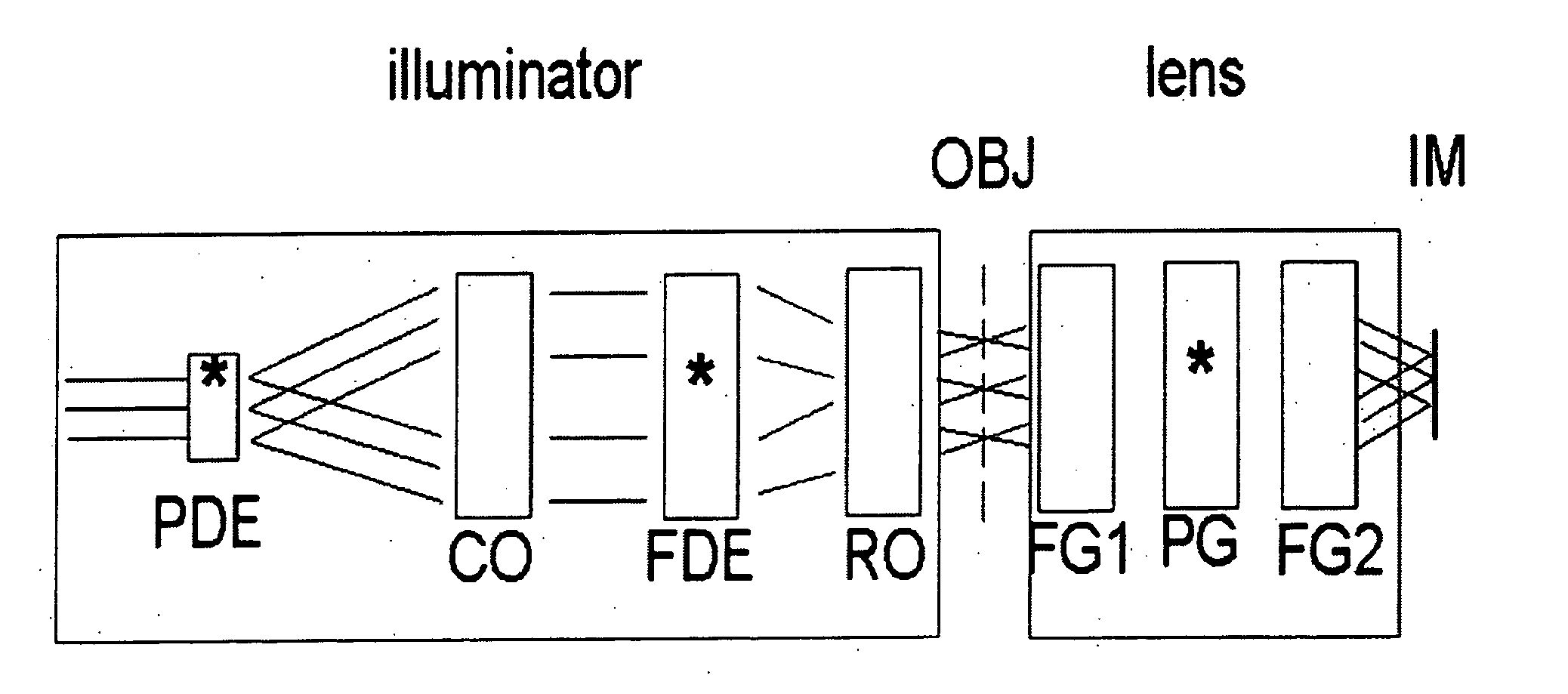
[0024] In an embodiment, the present invention provides a photon sieve provided as a pupil defining element or a field defining element in the illumination system IL of the apparatus as shown in FIG. 1 and 2. In an alternative embodiment, there is provided a photon sieve in the projection system, acting as a pupil lens element. In an alternative embodiment, the pupil lens element in the shape of a photon sieve is used for color correction of the radiation beam being projected. As a further embodiment, the photon sieve may be used as a transmitting diffracting element for EUV radiation.

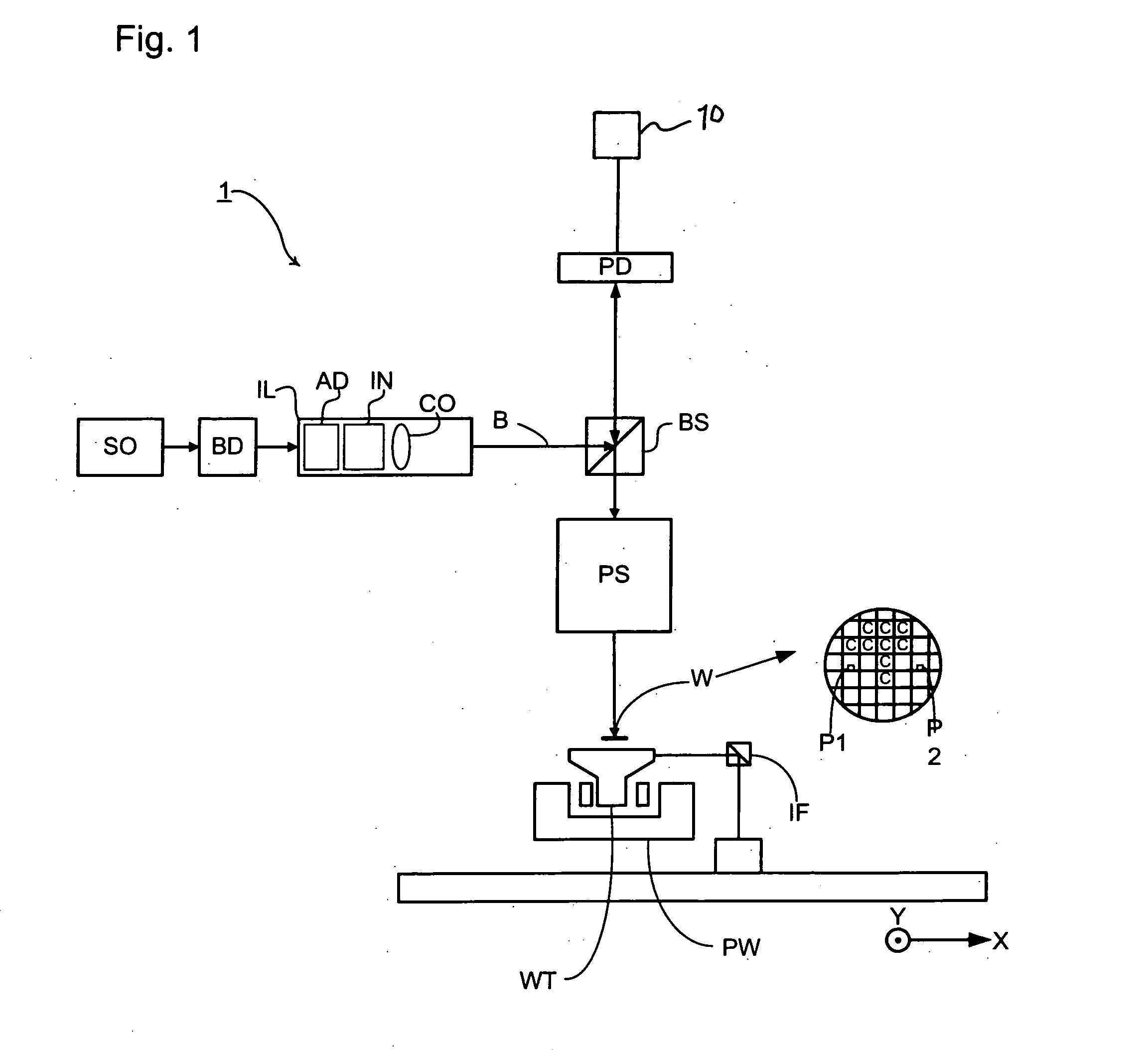
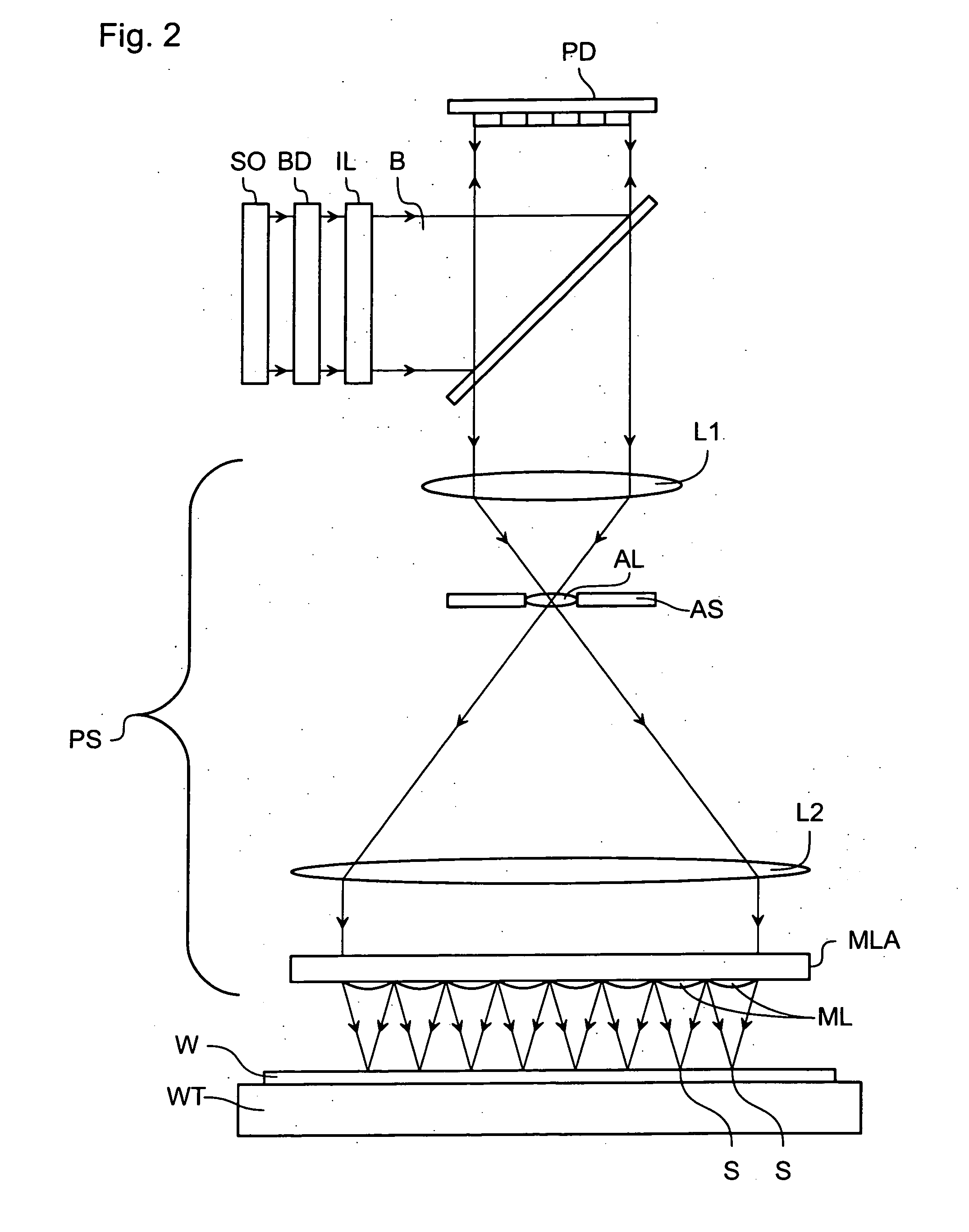
[0025]FIG. 1 schematically depicts a lithographic apparatus 1 according to an embodiment of the invention. The apparatus includes an illumination system (illuminator) IL configured to condition a radiation beam B (e.g. UV radiation). A patterning device PD (e.g. an array of individually controllable elements) that modulates the beam. In general, the position of the array of individually controllable e...


PUM


Abstract

The use of photon sieves may be as a pupil defining element in an illumination system; a field of defining elements in an illumination system; a pupil lens element in a projection lens; a color correction system in the projection system; or as a transmitting diffractive element for EUV.

Description

BACKGROUND OF THE INVENTION [0001] 1. Field of the Invention [0002] The present invention relates to an optical system in a lithographic apparatus and a method for manufacturing a device. [0003] 2. Description of the Related Art [0004] A lithographic apparatus is a machine that applies a desired pattern onto a substrate or part of a substrate. A lithographic apparatus may be used, for example. in the manufacture of flat panel displays, integrated circuits (ICs) and other devices involving fine structures. In a conventional apparatus, a patterning device, which may be referred to as a mask or a reticle, may be used to generate a circuit pattern corresponding to an individual layer of a flat panel display (or other device). This pattern may be transferred on (part of) the substrate (e.g. a glass plate), e.g. via imaging onto a layer of radiation-sensitive material (resist) provided on the substrate. [0005] Instead of a circuit pattern, the patterning device may be used to generate oth...

Claims


Application Information

Patent Timeline
IPC IPC(8): G01J3/10
CPCG03F7/70091G03F7/70108G03F7/70158G03F7/70575G03F7/7025G03F7/70308G03F7/70191
Inventor HUBERTUS MULKENS, JOHANNES
Owner ASML NETHERLANDS BV
Why Eureka
Try Eureka