DA converter, AD converter, and semiconductor device

a technology of ad converter and semiconductor device, which is applied in the direction of code conversion, instruments, television systems, etc., can solve the problems of reducing the variation of reference voltage, difficult to adjust the precision of analog gain, and difficult to perform fine adjustment with a precision of 12 bits or more, so as to achieve the effect of higher precision

Inactive Publication Date: 2007-08-23
SONY CORP
View PDF4 Cites 94 Cited by
  • Summary
  • Abstract
  • Description
  • Claims
  • Application Information

AI Technical Summary

Benefits of technology

[0022] According to the present invention, the gain control is performed on the first DA conversion section obtaining the analog output on the basis of the gain-control output signal obtained by the second DA conversion section. The precision of the gain-control output signal generated by the second DA con

Problems solved by technology

However, it is difficult to adjust analog gain in terms of precision.
For example, it is difficult to perf

Method used


Image

  • DA converter, AD converter, and semiconductor device
  • DA converter, AD converter, and semiconductor device
  • DA converter, AD converter, and semiconductor device

Examples


Embodiment Construction

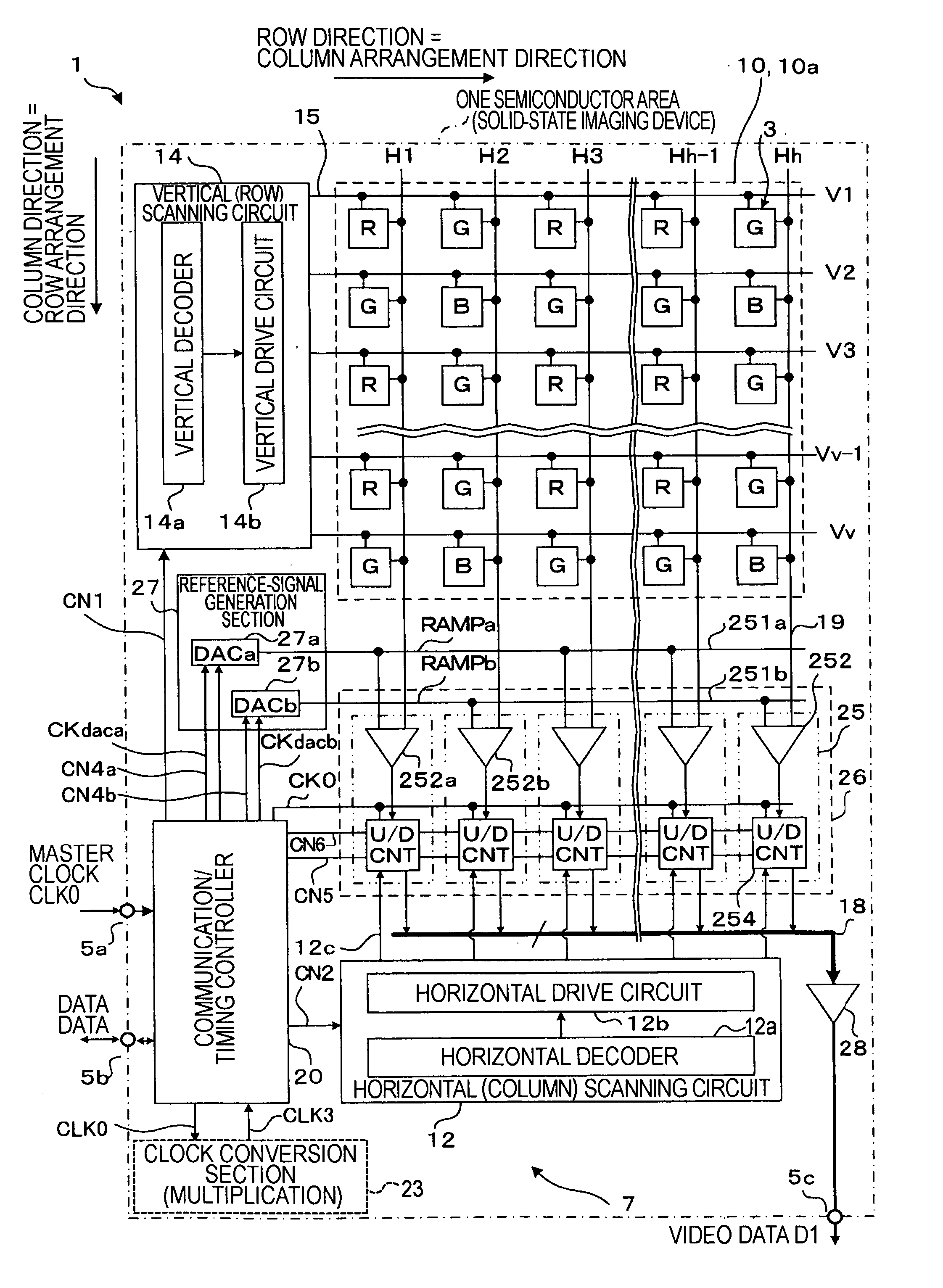
[0038] In the following, a detailed description will be given of an embodiment of the present invention with reference to the drawings. In this regard, a description will be given, in the below, of the case where the present invention is applied to a CMOS imaging device, which is an example of a solid-state imaging device of an X-Y addressing type. Also, a description will be given assuming that a CMOS imaging device includes all the pixels made of NMOSs or PMOSs.

[0039] However, this is only an example, and the device to be the target is not limited to a MOS imaging device. All the embodiments described below can be applied in the same manner to all semiconductor devices for detecting a physical-quantity distribution, in which a plurality of unit components having sensitivity to electromagnetic waves input from the outside, such as light, radiation rays, etc., are arranged in line or in a matrix.

Structure of Solid-State Imaging Device

[0040]FIG. 1 is a schematic configuration dia...


PUM


Abstract

A DA converter includes a first DA conversion section for obtaining an analog output signal in accordance with a digital input signal value, and a second DA conversion section for obtaining an analog gain control output signal in accordance with a digital gain control input signal value. In the DA converter, the gain control of the analog output signal generated by the first DA conversion section is performed on the basis of the gain control output signal generated by the second DA conversion section.

Description

CROSS REFERENCES TO RELATED APPLICATIONS [0001] The present invention contains subject matter related to Japanese Patent Application JP 2005-239686 filed in the Japanese Patent Office on Aug. 22, 2005, the entire contents of which are incorporated herein by reference. BACKGROUND OF THE INVENTION [0002] 1. Field of the Invention [0003] The present invention relates a DA (Digital-to-Analog) converter for converting a digital signal into an analog signal, an AD converter including the DA converter, and a semiconductor device such as an imaging device, etc. The present invention relates to, for example, a mechanism of a DA conversion using a current-source cell matrix having an array of cells arranged in a matrix. [0004] 2. Description of the Related Art [0005] DA converters for converting a digital signal into an analog signal are used in various ways in electronic apparatuses, for example, cameras or cell phones, or in semiconductor devices. [0006] For example, a semiconductor device ...

Claims


Application Information

Patent Timeline
IPC IPC(8): H03M1/66H03M1/56H03M1/68H03M1/70H04N5/335H04N5/376H04N5/378
CPCH03M1/1014H04N5/378H03M1/66H03M1/742H04N25/75
Inventor ASAYAMA, GOFUKUSHIMA, NORIYUKINITTA, YOSHIKAZUMURAMATSU, YOSHINORIAMANO, KIYOTAKA
Owner SONY CORP
Why Eureka
Try Eureka