Non-Volatile Memory Devices that Utilize Mirror-Image Programming Techniques to Inhibit Program Coupling Noise and Methods of Programming Same

a non-volatile memory device and programming technique technology, applied in static storage, digital storage, instruments, etc., can solve problems such as 3-bit data errors, and achieve the effect of reducing coupling noise and improving data storage reliability

Active Publication Date: 2007-08-23
SAMSUNG ELECTRONICS CO LTD
View PDF8 Cites 23 Cited by
  • Summary
  • Abstract
  • Description
  • Claims
  • Application Information

AI Technical Summary

Benefits of technology

[0009]Embodiments of the present invention include non-volatile memory devices having improved data storage reliability resulting from mirror-image programming techniques that operate to reduce coupling noise between adjacent memory cells. According to some of these embodiments, a non-volatile memory device includes a memory array having a plurality of rows and columns of non-volatile memory cells therein. These memory cells may be three-state memory cells that can be paired to provide 3-bit data per pair. The memory cells may also be arranged in a NAND-type structure, with each pair of non-volatile memory cells sharing a common word line. In particular, the memory array includes at least one row of three-state memory cells therein that are grouped in pairs to provide 3-bit data storage. The at least one row includes a first pair of left and right non-volatile memory cells extending immediately adjacent a second pair of left and right non-volatile memory cells.

Problems solved by technology

Unfortunately, the use of 3-state EEPROM cells in the pair configuration of FIG. 3B may require the use of complex error detection and correction circuitry because any single cell failure will typically result in a corresponding 3-bit data error for both cells in the corresponding pair.

Method used


Image

  • Non-Volatile Memory Devices that Utilize Mirror-Image Programming Techniques to Inhibit Program Coupling Noise and Methods of Programming Same
  • Non-Volatile Memory Devices that Utilize Mirror-Image Programming Techniques to Inhibit Program Coupling Noise and Methods of Programming Same
  • Non-Volatile Memory Devices that Utilize Mirror-Image Programming Techniques to Inhibit Program Coupling Noise and Methods of Programming Same

Examples


Embodiment Construction

[0032]The present invention now will be described more fully herein with reference to the accompanying drawings, in which preferred embodiments of the invention are shown. This invention may, however, be embodied in many different forms and should not be construed as being limited to the embodiments set forth herein; rather, these embodiments are provided so that this disclosure will be thorough and complete, and will fully convey the scope of the invention to those skilled in the art. Like reference numerals refer to like elements throughout and signal lines and signals thereon may be referred to by the same reference characters. Signals may also be synchronized and / or undergo minor Boolean operations (e.g., inversion) without being considered different signals.

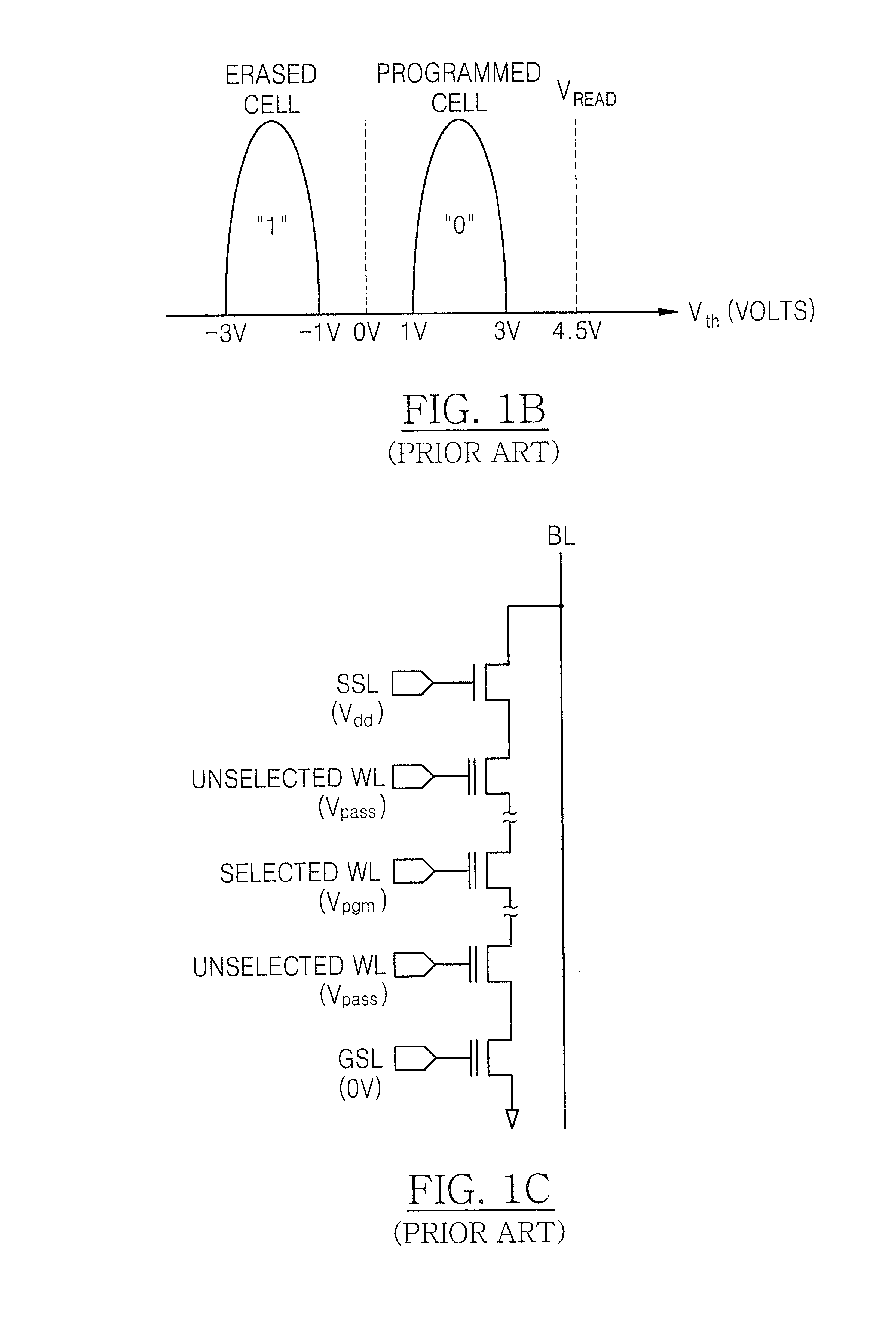
[0033]As shown in FIG. 4, a 3-level memory cell (MC) has three kinds of threshold voltage groups. The threshold voltage groups of the memory cells MCs can be classified based on a first reference voltage VR1 and a second ref...


PUM


Abstract

Non-volatile memory devices have improved data storage reliability resulting from mirror-image programming techniques that operate to reduce coupling noise between adjacent memory cells within a memory array. The adjacent memory cells include a first pair of memory cells and a second pair of memory cells. A program control circuit is provided to support mirror-image programming of the first and second pairs of memory cells when the two pairs of memory cells are storing the same 3-bit data.

Description

REFERENCE TO PRIORITY APPLICATION[0001]This application claims priority to Korean Application No. 2006-17142, filed Feb. 22, 2006, the disclosure of which is hereby incorporated herein by reference.FIELD OF THE INVENTION[0002]The present invention relates to integrated circuit memory devices and, more particularly, to nonvolatile memory devices and methods of programming nonvolatile memory devices.BACKGROUND OF THE INVENTION[0003]One class of nonvolatile memory devices includes electrically erasable programmable read only memory (EEPROM), which may be used in many applications including embedded applications and mass storage applications. In typical embedded applications, an EEPROM device may be used to provide code storage in personal computers or mobile phones, for example, where fast random access read times may be required. Typical mass storage applications include memory card applications requiring high capacity and low cost.[0004]One category of EEPROM devices includes NAND-ty...

Claims


Application Information

Patent Timeline
Patent Type & Authority Applications(United States)
IPC IPC(8): G11C16/04
CPCG11C11/5628G11C2216/14G11C16/0483G11C16/08G11C16/10G11C16/24
Inventor PARK, KI TAECHOI, JUNG DAL
Owner SAMSUNG ELECTRONICS CO LTD
Why Eureka
Try Eureka