
Semiconductor memory device for achieving high reliability without increasing process complexity and cost

a memory device and semiconductor technology, applied in the field of semiconductor memory devices, can solve the problems of holding characteristics, retention reliability, deterioration of tunnel oxide films, etc., and achieve the effects of improving data storage reliability of dram arrays, high reliability, and reducing the voltage level of the first bit lin

Inactive Publication Date: 2010-03-09
RENESAS ELECTRONICS CORP
View PDF8 Cites 4 Cited by
  • Summary
  • Abstract
  • Description
  • Claims
  • Application Information

AI Technical Summary

Benefits of technology

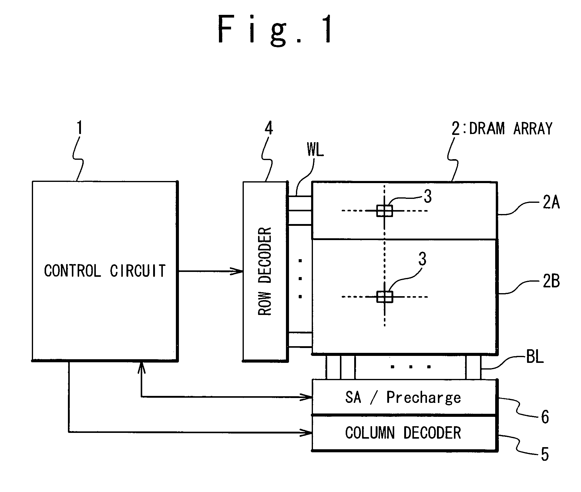
The present invention is a semiconductor memory device with a DRAM array and control circuit. The control circuit controls accesses to the DRAM array so that data hold characteristics of the first storage area are superior to those of the second storage area. This results in improved data retention reliability of the first storage area compared to the second storage area. The control circuit performs data accesses in units of access units each including multiple memory cells. The data access includes writing data to one memory cell and precharging the other memory cell. The sense amplifier identifies the data stored in the selected memory cell based on the difference between the voltage levels on the first and second bit lines. The present invention allows selectively improving data storage reliability of the DRAM array depending on the types of data to be stored without increasing the chip size and cost. The present invention can be implemented by selecting multiple word lines in the first storage area at the same time, even when all the memory cells have the same structure.

Problems solved by technology

For both types of the semiconductor memories, one of most important problems is improvement in data hold characteristics (that is, data retention reliability).
One issue for the flash memory is deterioration of the tunnel oxide film caused by repeated data write operations; the degradation of a tunnel oxide film makes it difficult to hold electrons and holes injected into the floating gate.
The deterioration of the data hold characteristics in the flash memory is generally caused by the degradation of the tunnel oxide film, and therefore, the deterioration of the data hold characteristics is an “irreversible change”.
As for the DRAM, on the other hand, data corruption is mainly caused by leakage of electric charges from cell capacitors, since cell data are stored as electric charges by the cell capacitors.
Nevertheless, the DRAM disclosed in this Laid Open Patent Application undesirably increases the complexity of the manufacture process, according to the investigation of the inventor of the present invention.
Integrating differently-shaped memory cells within a single chip undesirably decreases the manufacture process uniformity over the chip, and therefore increases the complexity of the manufacture process.

Method used


Image

  • Semiconductor memory device for achieving high reliability without increasing process complexity and cost
  • Semiconductor memory device for achieving high reliability without increasing process complexity and cost
  • Semiconductor memory device for achieving high reliability without increasing process complexity and cost

Examples


first embodiment

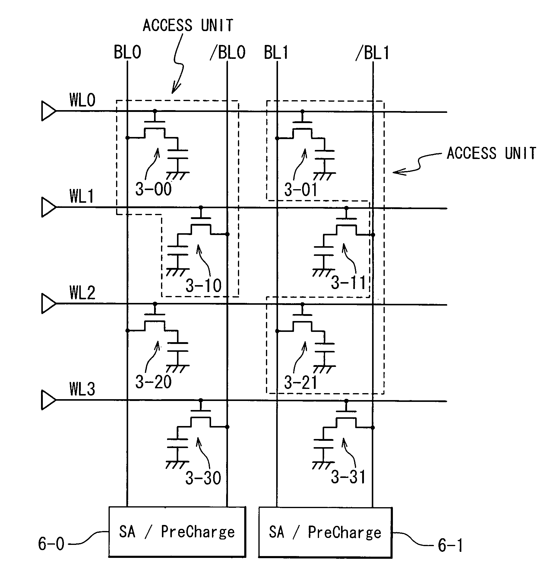
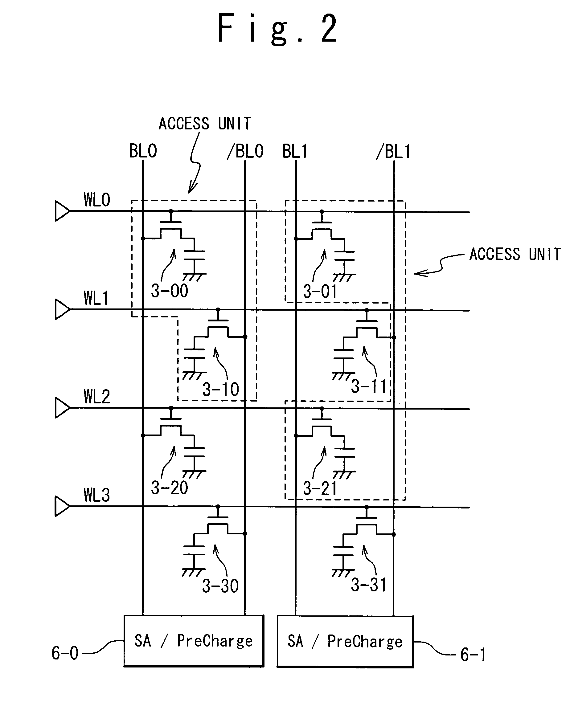
[0030]In a first embodiment, a set of n memory cells 3 (n is an integer of 2 or more) are regarded as one “access unit”, when data access is implemented to the first storage area 2A, in which high reliability is desired. Specifically, the control circuit 1 writes the same or complementary data into a set of n memory cells 3 belonging to the same access unit, and identifies data stored in the access unit on the basis of the electric charges accumulated in the set of n memory cells 3. When data access to the second storage area 2B is implemented, on the other hand, one single memory cell 3 is regarded as one “access unit”, as is the case of commonly-used DRAMs.

[0031]FIG. 2 is a circuit diagram partially illustrating the structure of the DRAM array 2 in the first storage area 2A, in which high reliability is desired. Word lines WL0 to WL3 and bit lines BL0, / BL0, BL1 and / BL1 are arranged to intersect with each other, and memory cells 3-00 to 3-31 are arranged at the respective interse...

second embodiment

[0046]FIG. 6 is a diagram illustrating a control method in a second embodiment. In the second embodiment, the control circuit 1 performs different refreshing controls with respect to the first storage area 2A and the second storage area 2B. Specifically, the control circuit 1 refreshes the memory cells within the second storage area 2B at a normal refresh cycle (e.g., 64 ms), while refreshing the memory cells within the first storage area 2A, in which the high reliability is required, at a shorter refresh cycle (e.g., 32 ms). In other words, the refreshing is implemented in the first storage area 2A more frequently than in the second storage area 2B. This allows the first storage area 2A to exhibit superior data hold characteristics, compared to those in the second storage area 2B.

[0047]Data refreshing at different refresh cycles may be performed as follows: In one embodiment, the memory cells within the first storage area 2A and the second storage area 2B are refreshed in parallel ...


PUM


Abstract

A semiconductor memory device is provided with a DRAM array and a control circuit. The DRAM array includes first and second storage areas. The control circuit controls an access to said DRAM array so that data hold characteristics of said first storage area are superior to those of said second storage area.

Description

BACKGROUND OF THE INVENTION[0001]1. Field of the Invention[0002]The present invention relates to a semiconductor memory device, more particularly, to a semiconductor memory device incorporating a DRAM (dynamic random access memory”) array and an operating method thereof.[0003]2. Description of the Related Art[0004]There are two types of semiconductor memories: a non-volatile memory such as a flash memory, and a volatile memory, such as a DRAM. For both types of the semiconductor memories, one of most important problems is improvement in data hold characteristics (that is, data retention reliability). Factors affecting on data hold characteristics depend on the type of memory.[0005]One issue for the flash memory is deterioration of the tunnel oxide film caused by repeated data write operations; the degradation of a tunnel oxide film makes it difficult to hold electrons and holes injected into the floating gate. The deterioration of the data hold characteristics in the flash memory is...

Claims


Application Information

Patent Timeline
Patent Type & Authority Patents(United States)
IPC IPC(8): G11C11/24
CPCG11C11/406G11C11/40622G11C2211/4061
Inventor TAKAHASHI, HIROYUKI
Owner RENESAS ELECTRONICS CORP
Learn More