Method of providing a via opening in a dielectric film of a thin film capacitor

a dielectric film and capacitor technology, applied in the direction of fixed capacitors, thin/thick film capacitors, fixed capacitor details, etc., can solve the problems of limiting the operational capabilities of passive components, substrate scalability, and even wet etching processes previously sought to be used, etc., to achieve the effect of reliably penetration through the high-k ceramic material of tfc lamina

Inactive Publication Date: 2007-08-30
INTEL CORP
View PDF8 Cites 9 Cited by
  • Summary
  • Abstract
  • Description
  • Claims
  • Application Information

AI Technical Summary

Problems solved by technology

Restricting the location of the passive components to the substrate's surface however can limit the passive components' operational capabilities (due to their inherent distance from the semiconductor device) and the substrate's scalability.
It has been found that CO2 laser processes or even wet etching processes previously sought to be used do not reliably penetrate through the high-k ceramic material of the TFC laminate.
However, use of the UV laser typically leads to thermal damage of the via edge regions (the damaged regions being called the “heat affected zone”) causing electrical shorting issues in the TFC, thereby impacting the functionality of the final package that includes the TFC.

Method used


Image

  • Method of providing a via opening in a dielectric film of a thin film capacitor
  • Method of providing a via opening in a dielectric film of a thin film capacitor
  • Method of providing a via opening in a dielectric film of a thin film capacitor

Examples


Embodiment Construction

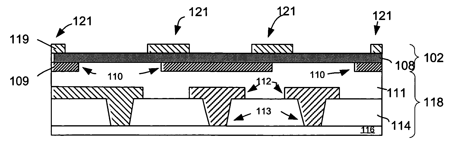
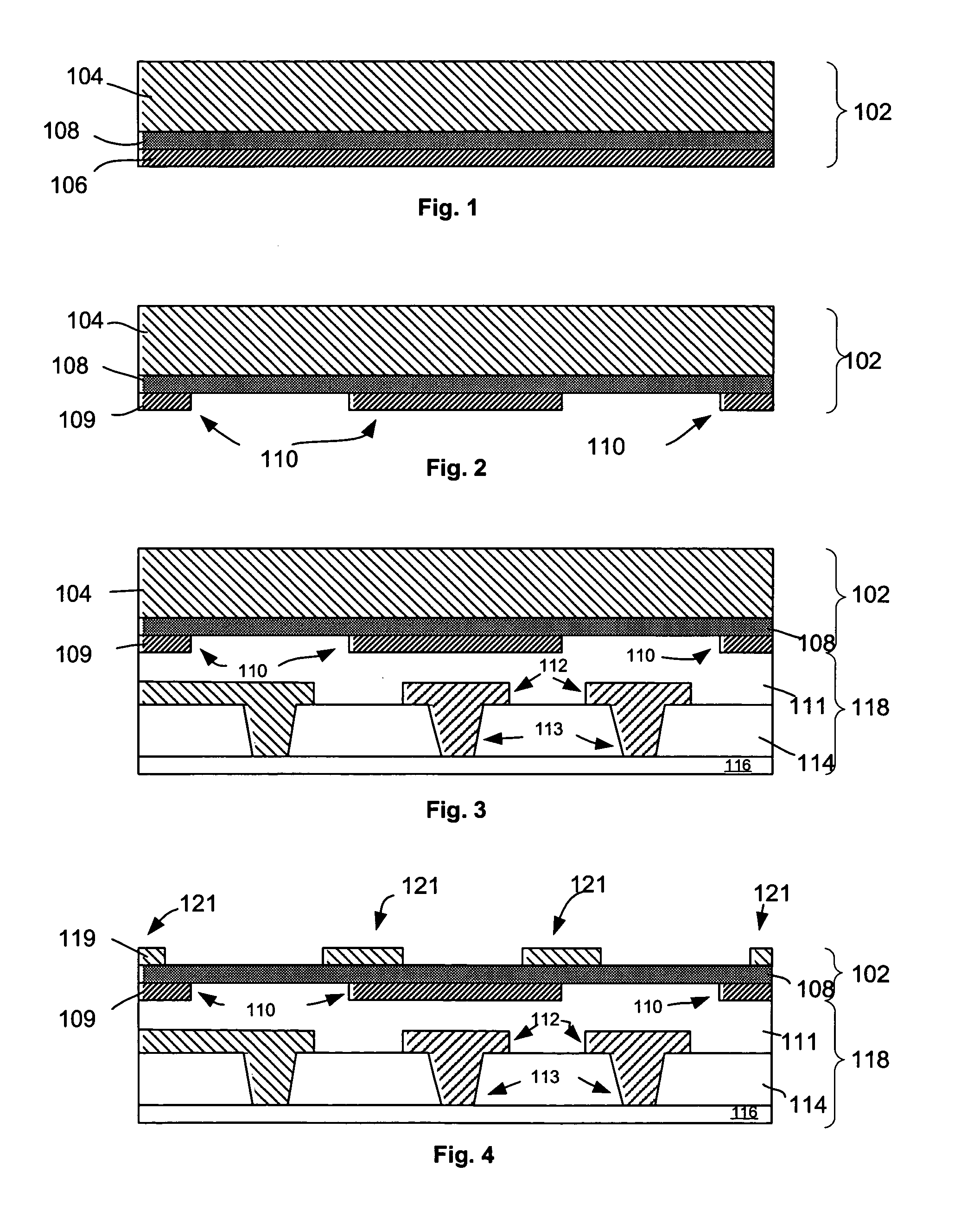
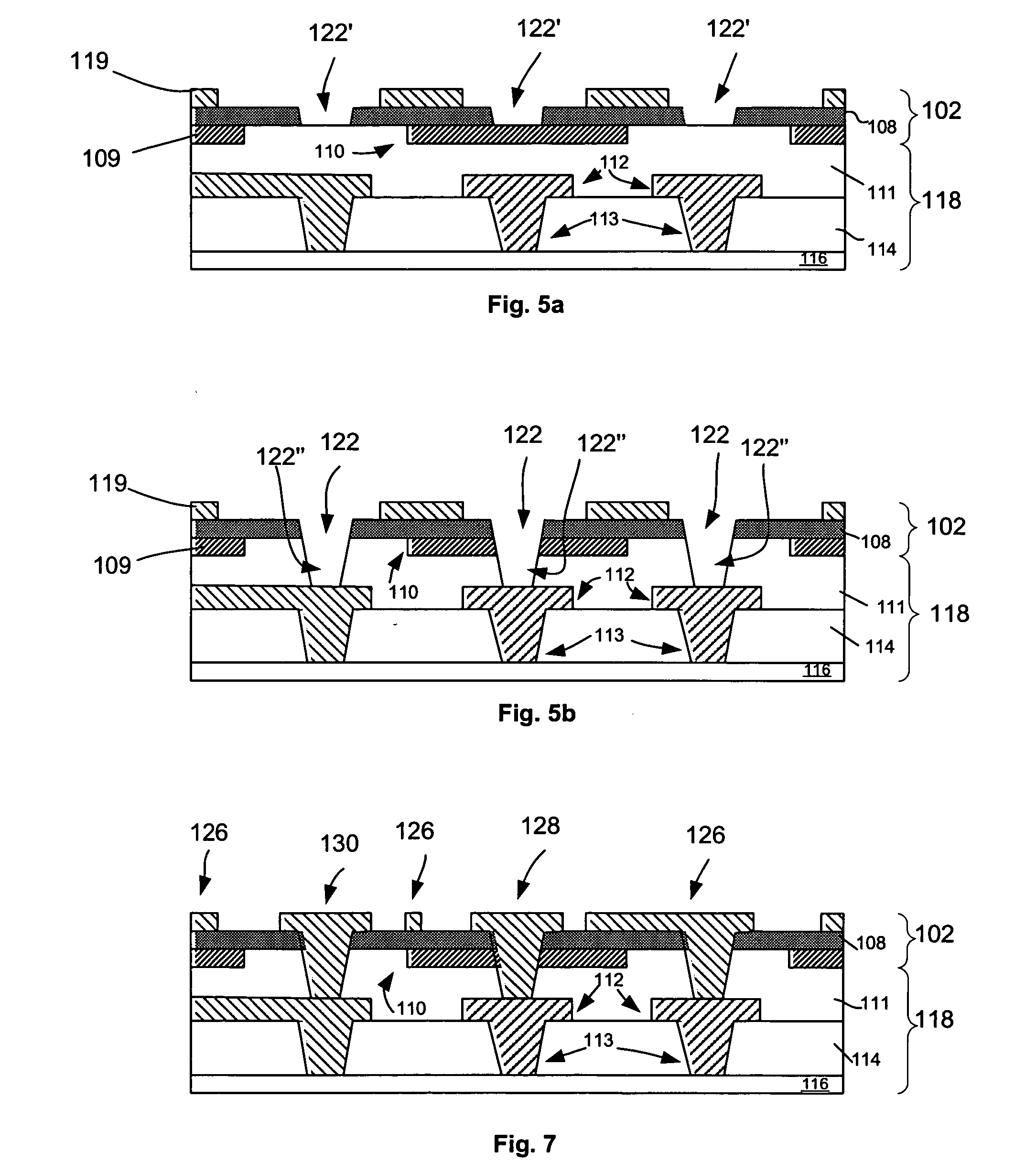
[0009] In the following detailed description, an embedded passive structure and its method of formation are disclosed. Reference is made to the accompanying drawings within which are shown, by way of illustration, specific embodiments by which the present invention may be practiced. It is to be understood that other embodiments may exist and that other structural changes may be made without departing from the scope and spirit of the present invention.

[0010] The terms on, above, below, and adjacent as used herein refer to the position of one layer or element relative to other layers or elements. As such, a first element disposed on, above, or below a second element may be directly in contact with the second element or it may include one or more intervening elements. In addition, a first element disposed next to or adjacent a second element may be directly in contact with the second element or it may include one or more intervening elements.

[0011] In one embodiment, a thin film lami...


PUM

PropertyMeasurementUnit
particle sizeaaaaaaaaaa
velocityaaaaaaaaaa

Abstract

An embedded passive structure, its method of formation, and its integration onto a substrate during fabrication are disclosed. A method comprises providing a thin film capacitor laminate that comprises: a high-k ceramic dielectric film; a conductive film disposed on one side of the high-k ceramic dielectric film; and a first electrode layer including first conductive portions disposed on another side of the high-k ceramic dielectric film. The method further comprises providing through via openings in the high-k ceramic dielectric film using powder blasting; and patterning the conductive film to yield a intermediate second electrode layer including intermediate second conductive portions disposed on the one side of the high-k ceramic dielectric film.

Description

FIELD OF THE INVENTION [0001] Embodiments of the present invention relate generally to methods of providing via openings adapted to be used for vias in a microelectronic package. BACKGROUND OF THE INVENTION [0002] The demand for increased mobility in consumer electronics is pressuring manufacturers to scale electronic technologies (e.g., semiconductor devices) to ever smaller dimensions. At the same time, the demand for increased functionality, speed, noise elimination, etc., is forcing manufactures to increase the number of passive components (e.g., capacitors and resistors) used by consumer electronic devices. Passive component integration has traditionally been accomplished by mounting them onto package and / or printed circuit board (PCB) substrate surfaces. Restricting the location of the passive components to the substrate's surface however can limit the passive components' operational capabilities (due to their inherent distance from the semiconductor device) and the substrate'...

Claims


Application Information

Patent Timeline
Patent Type & Authority Applications(United States)
IPC IPC(8): H01L21/20
CPCH01L2224/16H01L2924/01078H01L2924/15311H01G4/1227H01L2924/01019H01G4/33H01L21/486H01L28/55H01G4/228
Inventor MIN, YONGKI
Owner INTEL CORP
Why Eureka
Try Eureka