
Electrostatic discharge protection device in integrated circuit

a protection device and integrated circuit technology, applied in the direction of semiconductor devices, electrical equipment, transistors, etc., can solve the problems of secondary breakdown of the protection device itself, and insufficient increase of retained voltage vh

Inactive Publication Date: 2007-09-13
PANASONIC CORP
View PDF9 Cites 23 Cited by
  • Summary
  • Abstract
  • Description
  • Claims
  • Application Information

AI Technical Summary

Benefits of technology

[0015]Therefore, a main object of the present invention is to provide an ESD protection device that can be prevented from secondary breakdown in such a manner that a retained voltage Vh is made to a higher voltage without depending on a value of a maximum operation voltage of an internal circuit.
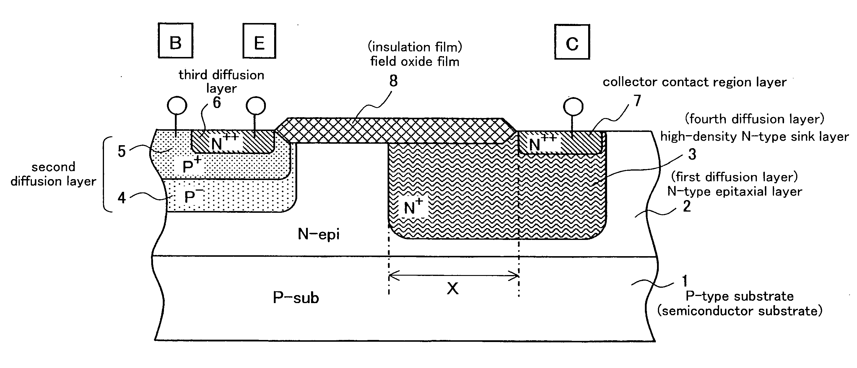
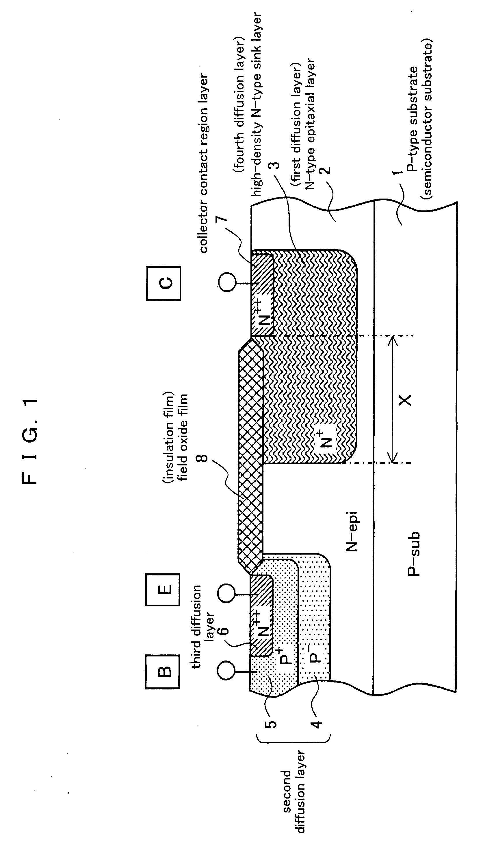
[0029]In the foregoing constitution, it is preferable that a fifth diffusion layer of the first conductivity type is formed in at least a part of the fourth diffusion layer below the insulation film. By doing this, a pinch resistor is formed in the region of the fourth diffusion layer below the fifth diffusion layer, and the pinch resistor is serially connected to the collector of the transistor. Even when it is desirable to obtain the higher retained voltage Vh, therefore, the retained voltage Vh can be further increased by changing the width of the fifth diffusion layer without any increase of the width of the fourth diffusion layer region itself (without any increase of a cell area). It is preferable that the fifth diffusion layer is provided in the fourth diffusion layer. Accordingly, a punch-through is formed through the fifth diffusion layer and the second diffusion layer, and the withstand voltage between the collector and base can be prevented from decreasing.
[0032]Further, the fifth diffusion layer of the first conductivity type is additionally formed in the fourth diffusion layer below the insulation film, so that the retained voltage Vh can be further increased without any increase of the area.

Problems solved by technology

It is because an excessive amount of current supply flows from the power supply of the internal circuit to the ESD protection device of the NPN transistor type and thereby the secondary breakdown of the ESD protection device of the NPY transistor type is caused due to the heat generated therein if the retained voltage Vh is reduced to be lower than the maximum operation voltage of the internal circuit.
However, the increase of the retained voltage Vh is still insufficient, and the protection device can be used only in a limited voltage range.
Therefore, the retained voltage of the ESD protection device of the NPN-transistor type may be lower than the maximum operation voltage in the integrated circuit having a high voltage resistance, which unfavorably results in the secondary breakdown of the protection device itself.

Method used


Image

  • Electrostatic discharge protection device in integrated circuit
  • Electrostatic discharge protection device in integrated circuit
  • Electrostatic discharge protection device in integrated circuit

Examples


embodiment 1

Preferred Embodiment 1

[0044]FIG. 1 is a sectional view showing a structure of an electrostatic discharge (ESD) protection device according to a preferred embodiment 1 of the present invention. The ESD protection device is suitable for providing an ESD protection to an internal circuit having a maximum operation voltage 40 V. As shown in FIG. 1, an N-type epitaxial layer 2 is formed on a P-type substrate 1 as a semiconductor substrate of a first conductivity type. The N-type epitaxial layer 2 is a first diffusion layer of a second conductivity type and serves as a collector. A high-density N-type sink layer 3 is formed from a surface of the N-type epitaxial layer 2 to inside thereof. The high-density N-type sink layer 3 is a fourth diffusion layer of the second conductivity type and serves as a collector layer. The high-density N-type sink layer 3 is formed with a density higher than that of the N-type epitaxial layer 2. A P− layer 4 and a P+ layer 5 are formed in a region of the N-t...

second preferred embodiment 2

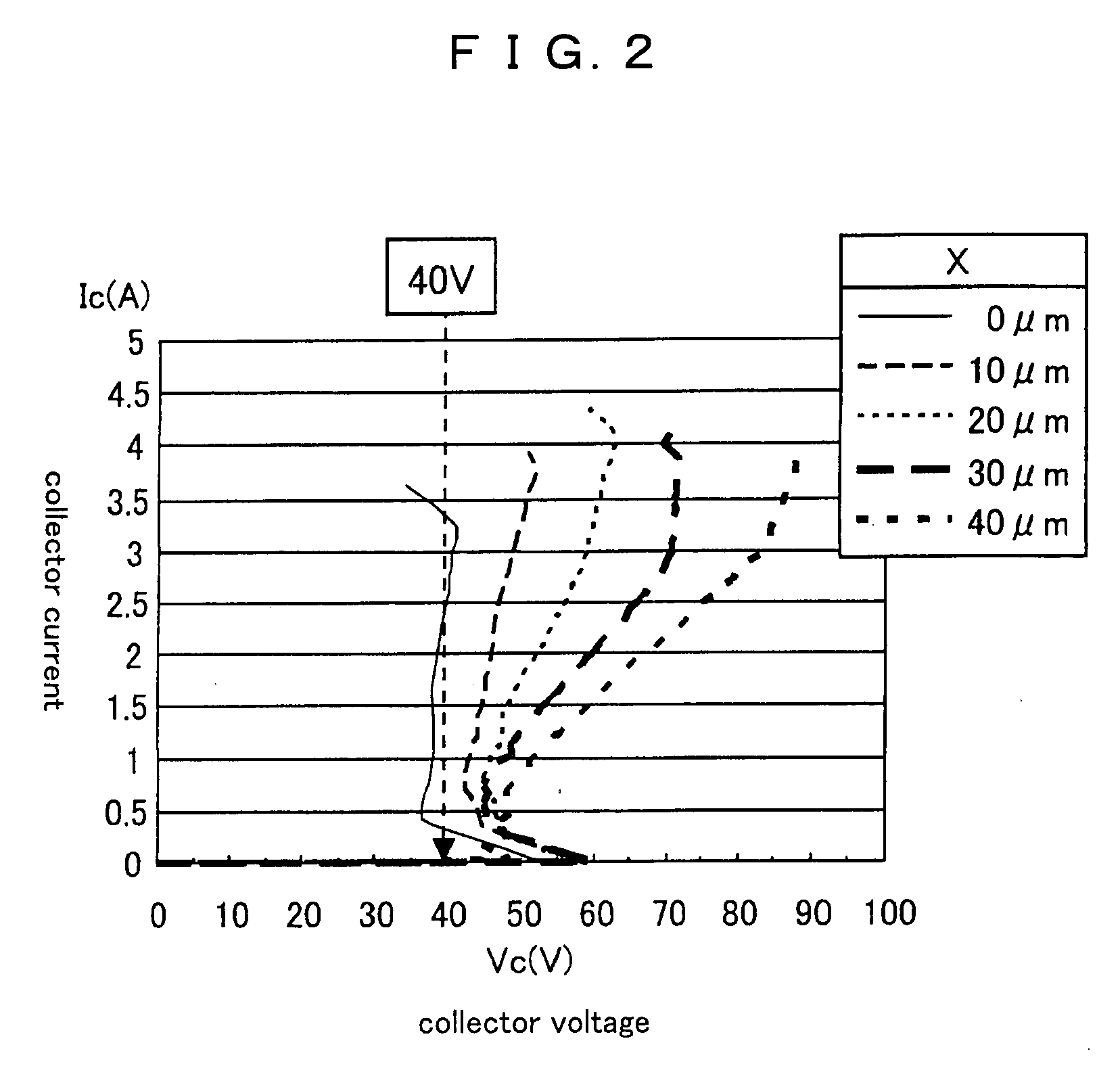
[0053]In the preferred embodiment 1, improvement of the retained voltage Vh is tried by expanding the region width X of the high-density N-type sink layer 3 below the field oxide film 8. However, it is necessary to set the region width X to at least 10 μm in order to be secured of the retain voltage Vh of at least 40 V as shown in FIG. 2.

[0054]In the case where use of the ESD protection device is desired in the range of higher voltages, it is necessary to further broaden the region width X. When use of the ESD protection device is tried in the region of the power-supply voltage of 50V, for example, it is necessary for the region width X to be at least 50 μm, which means that the cell area of the ESD protection device is increased to at least 50 μm in the horizontal direction. Therefore, the area of the ESD protection device occupied in the entire area of the chip is increased, and the chip size may be unfavorably increased in the constitution according to the preferred embodiment 1....


PUM


Abstract

An electrostatic discharge protection device of a semiconductor integrated circuit, comprising a first diffusion layer that is a diffusion layer of a second conductivity type provided on a semiconductor substrate of a first conductivity type and serves as a collector, a second diffusion layer that is a diffusion layer of the first conductivity type provided in the first diffusion layer and serves as a base, a third diffusion layer that is a diffusion layer of the second conductivity type provided in the second diffusion layer and serves as an emitter, a collector contact region provided in the first diffusion layer, a fourth diffusion layer that is a diffusion layer of the second conductivity type provided in the first diffusion layer in a downward region of the collector contact region in a substrate-thickness direction, wherein the fourth diffusion layer is formed shallower in a depth than that of the first diffusion layer in the substrate-thickness direction, deeper in a depth than that of the second diffusion layer in the substrate-thickness direction and with a high density than that of the first diffusion layer, and an insulation film formed on a surface of the first diffusion layer between the second diffusion layer and the collector contact region and serving as a field, wherein the fourth diffusion layer is extended up until a region below the insulation film.

Description

BACKGROUND OF THE INVENTION[0001]1. Field of the Invention[0002]The present invention relates to an electrostatic discharge protection device mainly in a bipolar or Bi-CMOS process.[0003]2. Description of the Related Art[0004]In order to protect an internal circuit in a semiconductor integrated circuit from breakdown due to static electricity charged in a human body, machine and the like, a semiconductor integrated circuit is conventionally provided with ESD (Electrostatic Discharge) protection circuit. The ESD protection circuit is described referring to FIG. 4.[0005]In the ESD protection circuit, a highest-potential-side diode 15 and a lowest-potential-side diode 16 are connected to an input / output terminal 12 of the semiconductor integrated circuit, and an ESD protection device 18 of NPN-transistor type is connected between a highest-potential terminal 13 and a lowest-potential terminal 14. When the lowest-potential terminal 14 is grounded and a plus surge is applied to the input...

Claims


Application Information

Patent Timeline
IPC IPC(8): H01L27/082H01L27/102
CPCH01L29/735H01L27/0259
Inventor NAWATE, MASAKATSUIMAHASHI, MANABU
Owner PANASONIC CORP
Learn More