Integrated optical waveform modulation

a technology of integrated optical waveform and modulation, which is applied in the direction of optics, electrical appliances, instruments, etc., can solve the problems of ttl logic being a relatively high-current and low-yield technology, using techniques that are not readily compatible with those of integrated circuits, and driving signals v(t) required to obtain satisfactory dynamic range of electro-optical components,

Active Publication Date: 2007-09-13
CIENA
View PDF3 Cites 58 Cited by
  • Summary
  • Abstract
  • Description
  • Claims
  • Application Information

AI Technical Summary

Benefits of technology

[0022] Thus, an aspect of the present invention provides a A method of modulating an optical carrier. A target carrier modulation is calculated based on an input data signal. An effective length of a control region of an optical modulator is then controlled based on the target carrier modulation.
[0023] Another aspect of the present inventio...

Problems solved by technology

However, electro-optical components such as MZ modulators are typically fabricated using techniques that are not readily compatible with those of integrated circuits (ICs).
Even where this is done, the drive signals V(t) required to obtain satisfactory dynamic range of the electro-optical component may significantly exceed the voltage and/or thermal limits of the IC.
It is also well known that TTL logic is a relatively high-current and low yield technology, which precludes its use in large integrated circuits with clock speeds higher than about 106 Hz.
In addition, the feedback loop used to linearize the sinusoidal response of the MZ modulator includes an inherent loop d...

Method used


Image

  • Integrated optical waveform modulation
  • Integrated optical waveform modulation
  • Integrated optical waveform modulation

Examples


Embodiment Construction

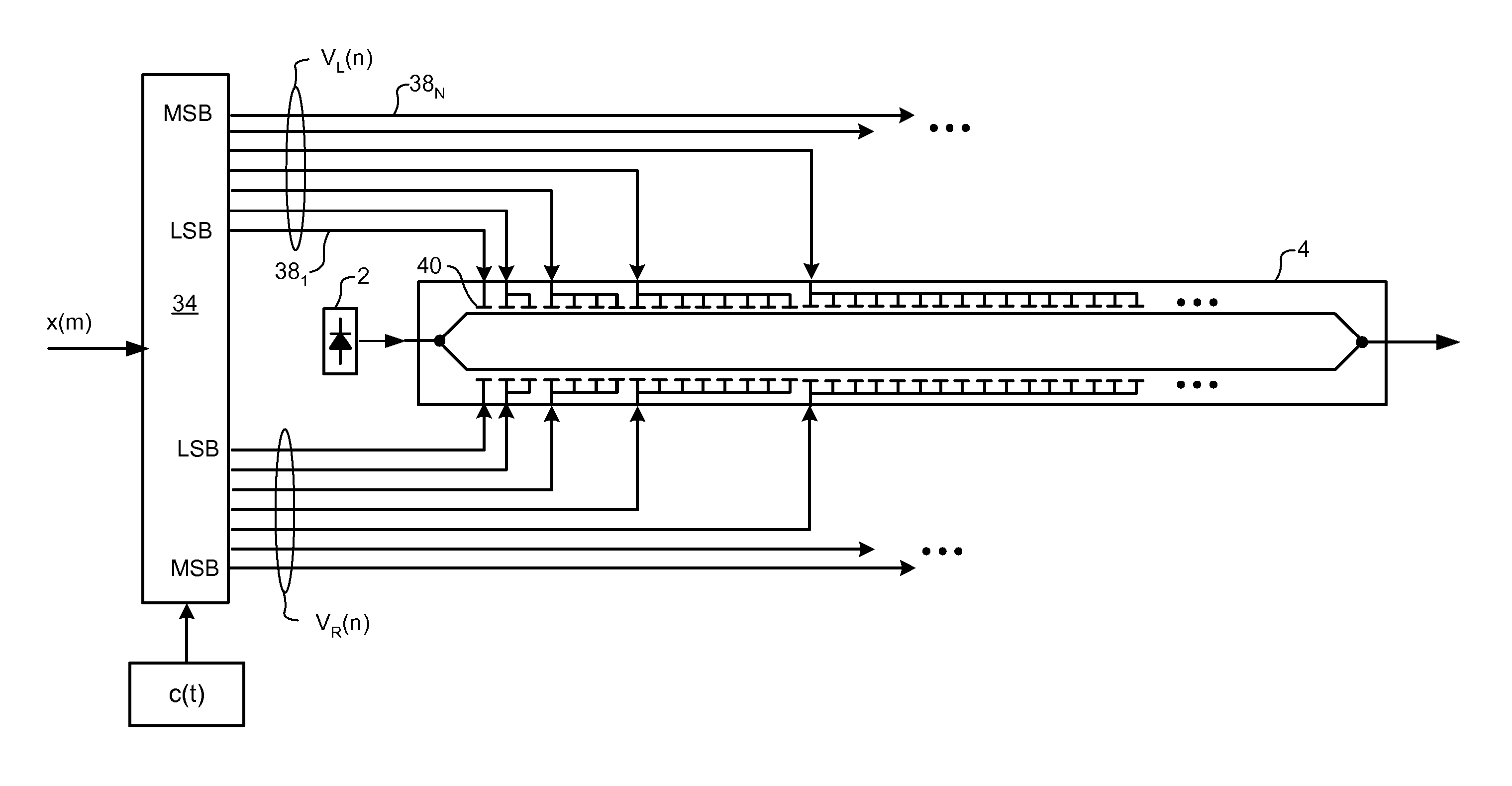
[0035] The present invention provides methods and apparatus for modulating the E-field of an optical carrier signal, in which the driver IC and the optical modulator can be integrated within a common package (i.e. co-packaged), either on a common substrate or on separate substrates closely coupled together. Embodiments of the invention are described below, by way of example only, with reference to FIGS. 4-7.

[0036] In general, the present invention operates by computing a target carrier modulation, and then varying the effective length of the control region 26 of the optical modulator in accordance with the target modulation. The electrodes of the modulator are configured such that the drive signals are the binary logic states output by the driver IC with no signal conditioning or power amplification required between the driver IC and the optical modulator. FIG. 4 illustrates a first representative embodiment of the present invention.

[0037] In the embodiment of FIG. 4, the driver I...


PUM


Abstract

A method of modulating an optical carrier. A target carrier modulation is computed based on an input data signal. An effective length of an optical modulator is then controlled based on the target carrier modulation.

Description

CROSS-REFERENCE TO RELATED APPLICATIONS [0001] This application is a divisional application of U.S. patent application Ser. No. 11 / 357,963 filed Feb. 22, 2006.MICROFICHE APPENDIX [0002] Not Applicable. TECHNICAL FIELD [0003] The present invention relates to optical signal transmitters for optical communications systems, and in particular to integrated optical waveform modulation. BACKGROUND OF THE INVENTION [0004] In the optical communications space, various techniques are used to synthesize an optical communications signal for transmission. A popular technique utilizes a laser 2 coupled to an external optical modulator 4, as shown in FIG. 1. The laser 2 generates a narrow-band continuous wave (CW) optical carrier signal 6 having a desired wavelength. The optical modulator 4 operates to modulate the amplitude and / or phase the carrier signal 6 to generate the optical communications signal 8 based on a drive signal 10 that encodes data to be transmitted. Typically, the drive signal 10...

Claims


Application Information

Patent Timeline
IPC IPC(8): H04B10/04
CPCG02F1/0121H04B10/505G02F1/225H04B10/548H04B10/5053
Inventor ROBERTS, KIMBELANGER, MICHEL
Owner CIENA
Why Eureka
Try Eureka