Lithographic type microelectronic spring structures with improved contours

a micro-electronic spring and contour technology, applied in the field of electric contact elements, can solve the problems of difficult to achieve the desired contact force, high manufacturing cost associated with manufacturing equipment and process time, and limited application range of fine-pitch spring contacts, etc., to achieve the effect of reducing the number of processing steps, and increasing the spring for

Inactive Publication Date: 2007-03-13
FORMFACTOR INC
View PDF87 Cites 61 Cited by
  • Summary
  • Abstract
  • Description
  • Claims
  • Application Information

AI Technical Summary

Benefits of technology

[0011]The present invention provides lithographically defined spring structures and methods to address the foregoing difficulties, while achieving adequate z-extension without requiring the use of multiple stepped lithographic layers. Lithographic type microelectronic spring contact structures are provided that are triangular in shape in plan view, low-aspect ratio rectangular in cross-section, and having z-component extension along a linear or curved slope. In particular, spring structures according to the present invention are suitable for being fabricated by depositing a layer of integrated spring material over a molded form, thereby greatly reducing the number of processing steps required. At the same time, the spring structures according to the present invention are contoured to provided numerous performance improvements. For example, structures having a U-shaped cross-section, a V-shaped cross-section, and / or a rib running along a length of the spring are provided. Such contouring provides spring structures with a higher stiffness and / or strength, thereby providing a higher spring force at the contact tip and / or working range for a given amount of spring material. The present invention additionally provides a lithographic type spring contact that is corrugated to increase its effective length and elastic range. Contouring of the spring structure according to the present invention further includes contouring in the plane of the substrate, to provide increased elastic range within a decreased footprint. The present invention further provides a variety of improved tips for making electrical contacts with lithographic type microelectronic spring structures.

Problems solved by technology

In practice, however, the cost of fabricating fine-pitch spring contacts has limited their range of applicability to less cost-sensitive applications.
Much of the fabrication cost is associated with manufacturing equipment and process time.
Consequently, it is difficult to achieve the desired contact force needed to make a reliable electrical contact at the contact tip, without exceeding the elastic range of the spring, and thereby potentially damaging it.
This also limits the elastic range of the spring, because the contact force is typically applied in the z direction.
However, the use of multiple layers adds undesirable cost and complexity to the manufacturing process.
Layered structures are also subject to undesirable stress concentration and stress corrosion cracking, because of the discontinuities (i.e., stepped structures) that result from layering processes.
The typical characteristics of very small feature size, relatively flat rectangular cross-section, and less z-component extension in proportion to spring length, make it very difficult to fabricate lithographically defined spring structures with adequate strength, stiffness, elastic range, and z-extension, to serve as reliable microelectronic spring contact structures.

Method used


Image

  • Lithographic type microelectronic spring structures with improved contours
  • Lithographic type microelectronic spring structures with improved contours
  • Lithographic type microelectronic spring structures with improved contours

Examples


Embodiment Construction

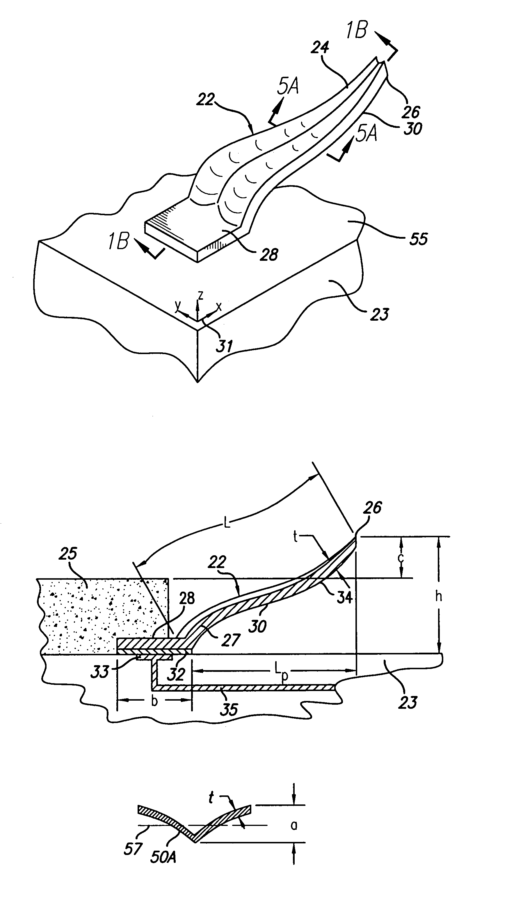
[0050]The present invention satisfies the need for microelectronic spring structure, that overcomes the limitations of prior art spring contacts. In the detailed description that follows, like element numerals are used to describe like elements illustrated in one or more figures. Various terms and acronyms are used throughout the detailed description, including the following:

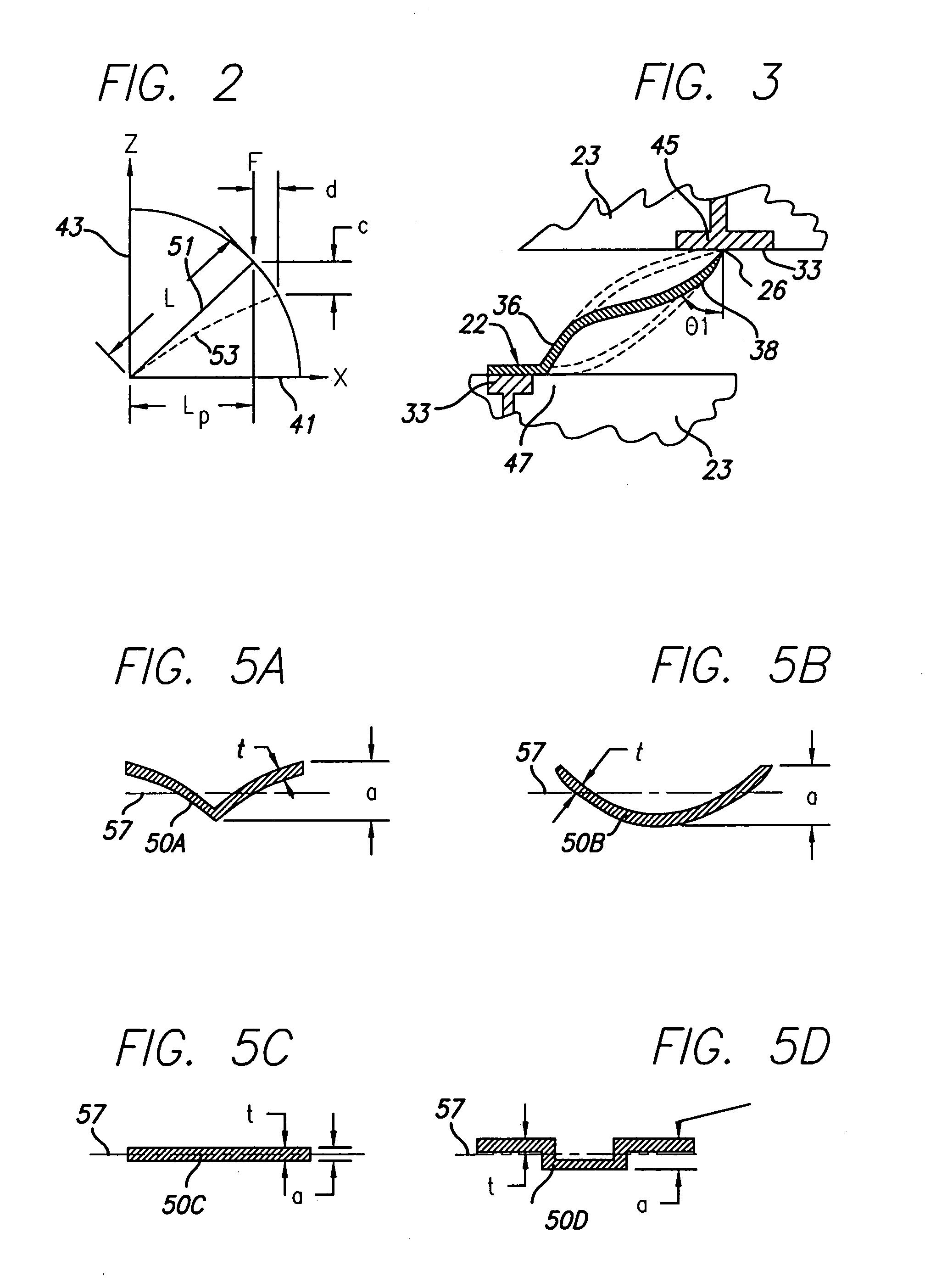
[0051]“Area moment of inertia,” sometimes denoted as “I,” is a section property defined as the integral of the section area times the distance from the neutral bending axis squared, that is:

∫z2dA

where z is the distance from the neutral axis of bending and dA is an element of the area being integrated. For example, for a rectangular cross-section having a width “w”, a thickness “t,” and a neutral axis through its centroid (½t) on the y-axis at z=0, the area moment of inertia is wt3 / 12.

[0052]“Contour,” when used as a verb, means to form a curved surface. When used as a noun, “contour” means a curved line defined ...


PUM

PropertyMeasurementUnit
heightaaaaaaaaaa
heightaaaaaaaaaa
widthaaaaaaaaaa

Abstract

Improved lithographic type microelectronic spring structures and methods are disclosed, for providing improved tip height over a substrate, an improved elastic range, increased strength and reliability, and increased spring rates. The improved structures are suitable for being formed from a single integrated layer (or series of layers) deposited over a molded sacrificial substrate, thus avoiding multiple stepped lithographic layers and reducing manufacturing costs. In particular, lithographic structures that are contoured in the z-direction are disclosed, for achieving the foregoing improvements. For example, structures having a U-shaped cross-section, a V-shaped cross-section, and / or one or more ribs running along a length of the spring are disclosed. The present invention additionally provides a lithographic type spring contact that is corrugated to increase its effective length and elastic range and to reduce its footprint over a substrate, and springs which are contoured in plan view. The present invention further provides combination (both series and parallel) electrical contacts tips for lithographic type microelectronic spring structures. The microelectronic spring structures according to the present invention are particularly useful for making very fine pitch arrays of electrical connectors for use with integrated circuits and other substrate-mounted electronic devices, because their performance characteristics are enhanced, while at the same time, they may be manufactured at greatly reduced costs compared to other lithographic type microelectronic spring structures.

Description

RELATED APPLICATION[0001]This application is a continuation-in-part of co-pending application Ser. No. 09 / 364,788, filed Jul. 30, 1999, entitled “INTERCONNECT ASSEMBLIES AND METHODS,” by Eldridge and Mathieu, which is incorporated by reference herein.BACKGROUND OF THE INVENTION[0002]1. Field of the Invention[0003]The present invention relates to electrical contact elements for electrical devices, and more particularly to lithographic type, microelectronic spring contacts with improved contours.[0004]2. Description of Related Art[0005]Recent technological advances, such as described in U.S. Pat. No. 5,917,707 to Khandros et al., have provided small, flexible and resilient microelectronic spring contacts for mounting directly to substrates, such as semiconductor chips. The '707 patent discloses microelectronic spring contacts that are made using a wire bonding process that involves bonding a very fine wire to a substrate, and subsequent electro-plating of the wire to form a resilient ...

Claims


Application Information

Patent Timeline
Patent Type & Authority Patents(United States)
IPC IPC(8): H01R12/10H01R12/61G01R1/067G01R1/073G01R3/00H01L21/768H01L23/48H01L23/482H05K3/40H05K7/10
CPCH01L23/4822H01L24/72H05K7/1069G01R1/06727G01R3/00G01R1/07342Y10T29/4922H01L2924/01012H01L2924/01013H01L2924/01027H01L2924/01029H01L2924/01042H01L2924/01046H01L2924/01049H01L2924/01074H01L2924/01078H01L2924/01079H01L2924/01082H01L2924/14H01L2924/19041H01L2924/30107H05K3/4092H01L2924/01006H01L2924/01019H01L2924/01023H01L2924/01033H01L2924/01047G01R1/06733Y10T29/49151
Inventor ELDRIDGE, BENJAMIN N.WENZEL, STUART W.
Owner FORMFACTOR INC
Why Eureka
Try Eureka