Semiconductor device having function of improved electrostatic discharge protection

a technology of electrostatic discharge protection and micro-conductor, which is applied in the direction of instruments, basic electric elements, and mechanical means, can solve the problems of small capacity of parasitic diodes within chips, relatively more difficult to protect esd, and significant damage to electronic devices by static electricity, so as to improve the pressure resistance against static electricity and improve the protection of protection diodes

Active Publication Date: 2007-09-20
SAMSUNG ELECTRONICS CO LTD
View PDF10 Cites 13 Cited by
  • Summary
  • Abstract
  • Description
  • Claims
  • Application Information

AI Technical Summary

Benefits of technology

[0033]In some exemplary embodiments of the invention, an electrostatic pressure resistance increases and thus an electrostatic discharge protection of protection diode may be improved. In addition, a load concentration to a connection part of the protection device is smoothened and dispersed, and thus the pressure resistance against static electricity is improved and further a contact connection structure having a durability against a wire bonding force may also be provided.

Problems solved by technology

However, static electricity may significantly damage electronic devices, including integrated-circuit chips.
However, the above silicide process may result in certain difficulties with regard to electrostatic discharge protection such as, the capacity of parasitic diodes within a chip may be small when using this process.
In other words, it may be relatively more difficult to protect the ESD in a semiconductor integrated circuit formed by a silicide process, and thus chip designers have been trying to obtain an improved ESD protection level.
Nevertheless, with the above-mentioned conventional semiconductor devices, a weakened portion for pressure resistance in a connected part between a pad and a protection device is also generated, which in turn may lead to an electrostatic breakdown in the semiconductor device.

Method used


Image

  • Semiconductor device having function of improved electrostatic discharge protection
  • Semiconductor device having function of improved electrostatic discharge protection
  • Semiconductor device having function of improved electrostatic discharge protection

Examples


Embodiment Construction

[0050]Exemplary embodiments of the present invention now will be described more fully hereinafter with reference to the accompanying drawings, in which exemplary embodiments of the invention are shown. This invention may, however, be embodied in many different forms and should not be construed as limited to the exemplary embodiments set forth herein. Rather these embodiments are provided so that this disclosure will be thorough and complete, and will fully convey the scope of the invention to those skilled in the art.

[0051]Hereinafter, exemplary embodiments of the present invention will be described in detail with reference to FIGS. 9 to 15 in which like reference characters refer to the same parts throughout the different views. It will be understood by those skilled in the art that the present invention can be embodied by numerous different types and is not limited to the following described exemplary embodiments. The following various embodiments are exemplary in nature.
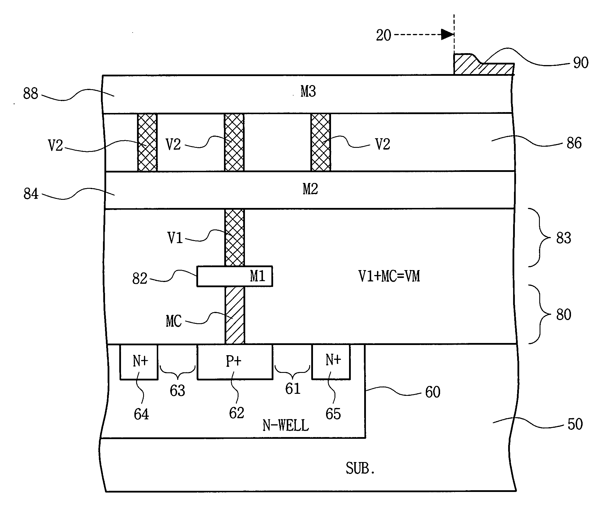
[0052]A c...


PUM

PropertyMeasurementUnit
electricallyaaaaaaaaaa
conductiveaaaaaaaaaa
voltageaaaaaaaaaa

Abstract

A semiconductor device includes a diode region having a plurality of protection diodes and a pad region overlapped with an upper part of the diode region. The pad region having a pad installed corresponding to an external connection terminal. The semiconductor device further includes a contact plug unit which connects at least one of a plurality of active regions constituting the diode region and the pad within the diode region.

Description

CROSS-REFERENCE TO RELATED APPLICATION[0001]This application claims priority from Korean Patent Application No. 10-2006-0024790, filed Mar. 17, 2006, the disclosure of which is hereby incorporated by reference herein in its entirety.TECHNICAL FIELD[0002]The present disclosure relates to semiconductor integrated circuits, and more particularly, to an electrical connection between pads and electrostatic discharge protection devices in a semiconductor integrated circuit.BACKGROUND[0003]Semiconductors devices are becoming more highly-integrated and are operating at increasingly higher clock speeds, thereby resulting in higher-performance electronic systems being produced. The above-mentioned higher-performance electronic systems include, for example, portable multimedia players, personal computers or electronic communication devices. Accordingly, manufacturers of integrated circuit chips are seeking to manufacture chip internal circuits according to a reduced critical dimension.[0004]Ho...

Claims


Application Information

Patent Timeline
Patent Type & Authority Applications(United States)
IPC IPC(8): H01L23/62
CPCH01L27/0255H01L2924/0002Y10T29/41H01L2924/00G01B3/1084G01B3/30
Inventor YANG, HYANG-JA
Owner SAMSUNG ELECTRONICS CO LTD
Why Eureka
Try Eureka