
Uniform impedance conducting lines for a liquid crystal display

Inactive Publication Date: 2007-09-20
HANNSTAR DISPLAY CORPORATION
View PDF2 Cites 48 Cited by
  • Summary
  • Abstract
  • Description
  • Claims
  • Application Information

AI Technical Summary

Benefits of technology

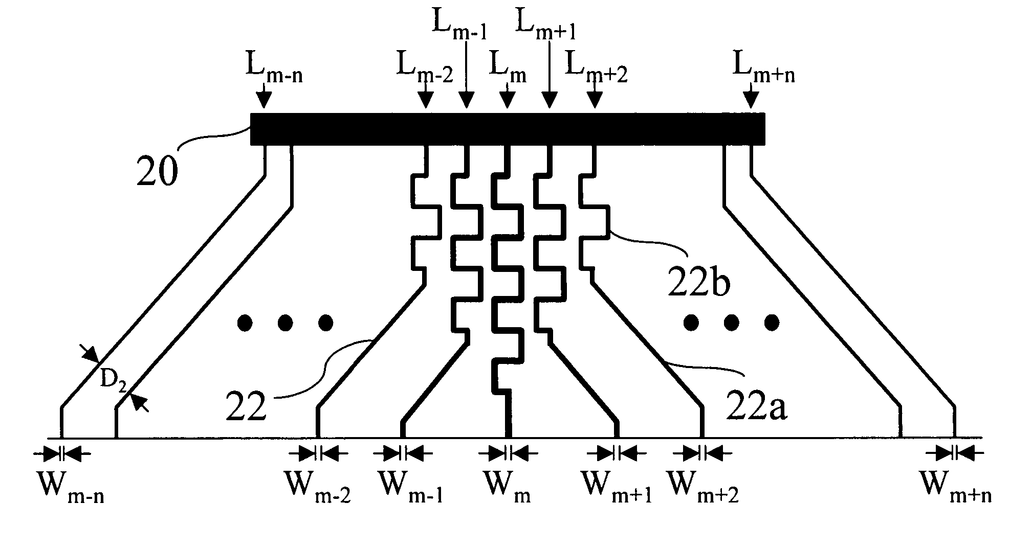
[0009] To achieve these and other advantages and in order to overcome the disadvantages of the conventional method in accordance with the purpose of the invention as embodied and broadly described herein, the present invention provides a conducting line design used in LCD panels, in which the lengths and widths of the conducting lines are made different to allow each line to have identical impedances. The plurality of conducting lines is formed in a fanlike shape and is used for transmitting control signals of the control integrated circuits (ICs) to the transistors. Each of the conducting comprises a respective width and a respective length. The width of the conducting lines increases towards the medial portion of the fanlike shape. Also, the length of the conducting lines increases towards the medial portion of the fanlike shape. The arrangement of the various lengths and widths make the resistance and capacitance of the conducting lines uniform.
[0010] An object of the present invention is to provide an LCD panel capable of producing high quality optical performance.
[0013] Since the conducting lines have uniform impedance, the optical performance is improved.

Problems solved by technology

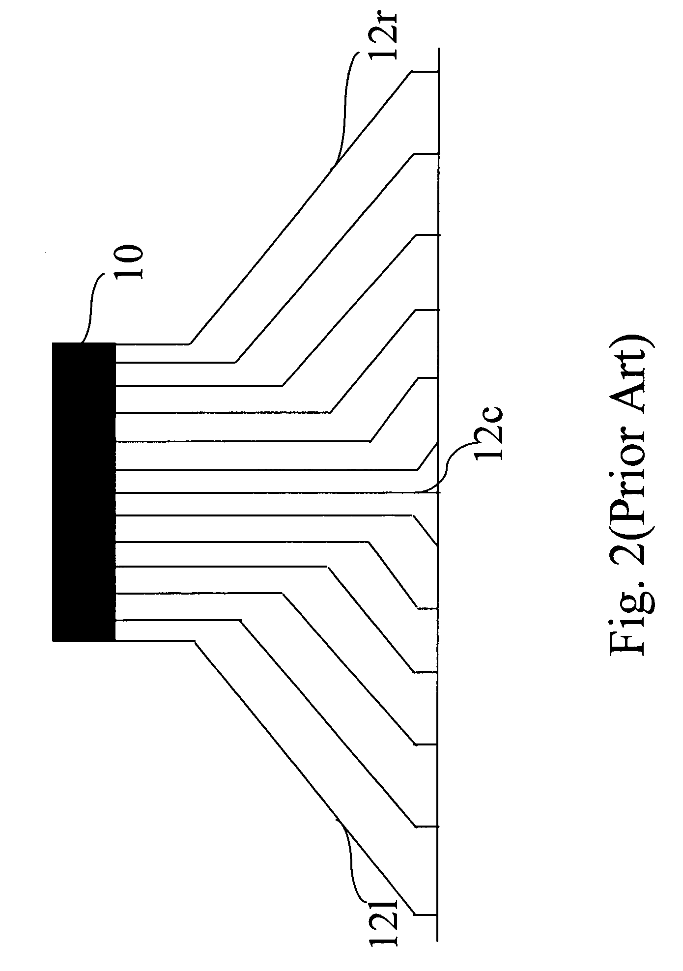
Because the active area of the two sides of the ICs is not enough, the design of longer and thicker conducting lines at the left and right sides will make the distance between conducting lines too close which easily results in shorting of the circuit, hence reducing the yield.

Method used


Image

  • Uniform impedance conducting lines for a liquid crystal display
  • Uniform impedance conducting lines for a liquid crystal display
  • Uniform impedance conducting lines for a liquid crystal display

Examples


Embodiment Construction

[0026] Reference will now be made in detail to the preferred embodiments of the present invention, examples of which are illustrated in the accompanying drawings. Wherever possible, the same reference numbers are used in the drawings and the description to refer to the same or like parts.

[0027] The present invention provides a conducting line design that makes the resistance and capacitance of each conducting line identical. Through change and proper combination of the length and width of each conducting line, the present invention allows the conducting lines to have the same electrical properties, thereby enhancing the image quality of the LCD panel.

[0028] The present invention makes use of impedance compensation to reduce the difference in resistance and capacitance between conducting lines. Refer to FIG. 5, which is a drawing illustrating the conducting lines according to an embodiment of the present invention. Each conducting line 22 comprises a first portion 22a and a second ...


PUM


Abstract

A liquid crystal display panel with a fanlike shaped conducting line design that provides uniform impedance is disclosed. The liquid crystal display panel comprises a plurality of transistors, a plurality of control ICs and a plurality of conducting lines. Each of the conducting lines comprises a respective width and a respective length. The width and length of the conducting lines increases towards the medial portion of the fanlike shape. The arrangement of the length and width makes the resistance and capacitance of the conducting lines uniform. As a result, the display panel achieves higher optical performance and improved quality.

Description

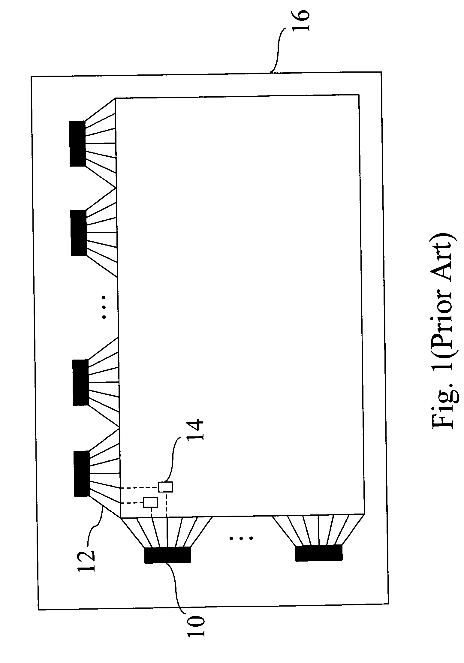
BACKGROUND OF THE INVENTION [0001] 1. Field of the Invention [0002] The present invention relates to a liquid crystal display panel and, more particularly, to a liquid crystal display panel whose conducting lines for transmitting control signals of the control integrated circuits have uniform resistance and capacitance. [0003] 2. Description of Related Art [0004] Liquid crystal displays (LCDs) have gradually replaced cathode ray tubes (CRTs) in the market, and have been more and more appreciated by consumers. Liquid crystal displays not only have the advantage of compactness, but also have lower power consumption. Therefore, they have occupied an important position in almost every field of their application. [0005] As shown in FIG. 1, a conventional LCD panel 16 has several control ICs 10 as its signal input terminals. Each control IC 10 is also connected to a plurality of conducting lines 12 for transmitting control signals to a plurality of transistors 14 arranged in an array. The...

Claims


Application Information

Patent Timeline
IPC IPC(8): G02F1/1345G02F1/1343
CPCG02F1/136286G02F1/13452
Inventor LIAO, CHIA-TECHUNG, TE-CHENG
Owner HANNSTAR DISPLAY CORPORATION
Learn More