Optical components array device, microlens array and process of fabricating thereof

a technology of optical components and microlens, which is applied in the direction of mountings, instruments, magnification glasses, etc., can solve the problems of high equipment cost and time consumption, high manufacturing cost, and shortcoming of photoresist reflow, etc., and achieve the effect of low cos

Inactive Publication Date: 2007-09-20
CHUNGHWA PICTURE TUBES LTD
View PDF8 Cites 52 Cited by
  • Summary
  • Abstract
  • Description
  • Claims
  • Application Information

AI Technical Summary

Benefits of technology

[0010] In view of the above, an object of the invention is to provide a low cost process of fabricating a microlens array.
[0012] Additionally, still another object of the invention is to provide an optical components array device having improved performance.
[0030] In view of the above, the invention adopts a self-assembled monolayer to change the surface property of the substrate, so as to form a hydrophilic region and a hydrophobic region. Thereafter, the liquid microlens are formed by condensing the liquid microlens material on the hydrophilic region under the surface tension. Therefore, it is possible to apply the process of the present invention in the mass production of the microlens array. The manufacturing cost of the microlens array can be effectively reduced.

Problems solved by technology

However, the disadvantages of ink-jet printing are the high equipment cost and time-consumption.
However, the shortcoming of the photoresist reflow is the expensive lithographic equipment and the complicated fabricating process.
However, the shortcoming of molding lies in the high manufacturing cost and it is difficult to miniaturize the microlens.
The shortcoming of mask lithography lies in that the half-tong mask has a high manufacturing cost and the complicated fabricating process.
The shortcoming of laser direct-writing lies in that the equipment of the excimer laser is expensive and small particles remaining on the surface of the work piece adversely affect the optical properties of the microlens.

Method used


Image

  • Optical components array device, microlens array and process of fabricating thereof
  • Optical components array device, microlens array and process of fabricating thereof
  • Optical components array device, microlens array and process of fabricating thereof

Examples


Embodiment Construction

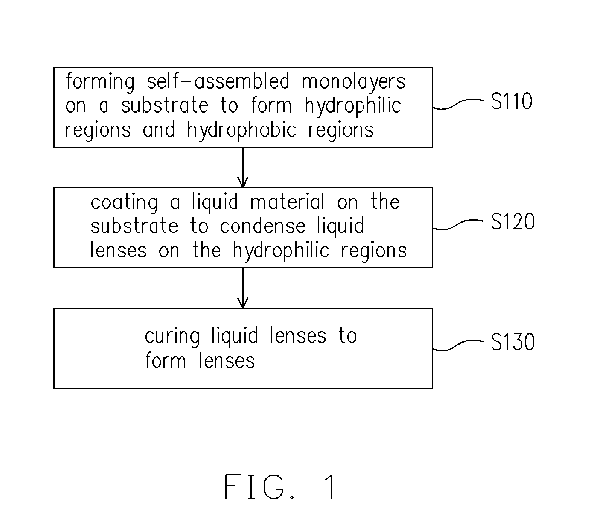
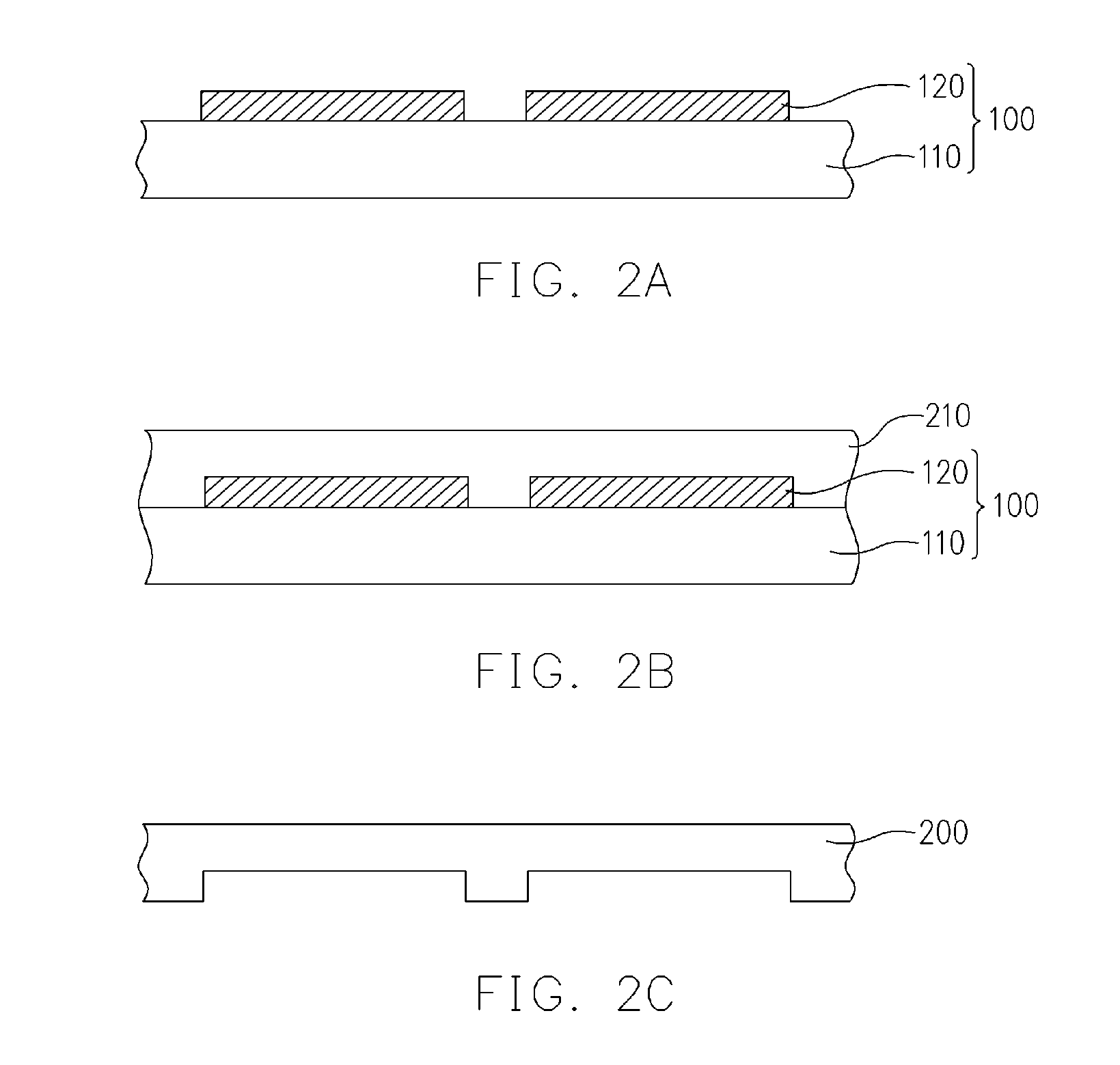
[0036]FIG. 1 is a flow chart of the process of fabricating the microlens array according to one embodiment of the invention. FIGS. 2A to 2G are sectional views showing the steps of the process of fabricating the microlens array according to one embodiment of the invention. Referring to FIG. 1, first, at Step S110, a self-assembled monolayer is formed on a substrate, so as to form a hydrophilic region and a hydrophobic region. Next, at Step S120, a liquid material is coated on the substrate, so as to condense multiple liquid microlens on the hydrophilic region. Next, a Step S130, the liquid microlens are cured so as to form a plurality of microlens

[0037] In the embodiment, the process of forming the self-assembled monolayer includes micro contact printing or other suitable methods.

[0038] Referring to FIG. 2A, in the micro contact printing, a first mould 100 having a substrate 110 and pillar structures 120 disposed thereon is provided. According to an embodiment of the present inven...


PUM


Abstract

A process of fabricating a microlens array is provided. A self-assembled monolayer is formed on a substrate to form a hydrophilic region and a hydrophobic region. A liquid material is coated on the substrate so that a plurality of liquid microlenses is condensed on the hydrophilic region. The liquid microlenses are cured to form a plurality of microlenses.

Description

BACKGROUND OF THE INVENTION [0001] 1. Field of Invention [0002] The present invention relates to an optical components array and a process of fabricating the same. More particularly, the present invention relates to a microlens array and a process of fabricating the same. [0003] 2. Description of Related Art [0004] Recently, the application of the microlens has attracted great attention, as the microlens can significantly improve the performance of photoelectronic devices, especially in the fields of light-emitting devices, photo-detectors, solar cells, optical fiber communication, and micro-optical-electromechanical system, and so on. The prior art has proposed to fabricate a microlens array on the surface of the light-emitting diode, raising 50% the light-outcoupling efficiency. The prior art has proposed to fabricate a microlens array on the surface of the photo-detector enhancing 11% of the photocurrent. The microlens array can also be used in the solar cells of the satellite im...

Claims


Application Information

Patent Timeline
Patent Type & Authority Applications(United States)
IPC IPC(8): G02B3/00
CPCG02B3/0018G02B3/0056G02B3/0031
Inventor HUANG, WEN-KUEIKO, CHU-JUNGCHEN, FANG-CHUNG
Owner CHUNGHWA PICTURE TUBES LTD
Why Eureka
Try Eureka